Fairchild FEB-L034 service manual

User Guide for
FEB-L034
Evaluation Board
Universal Line Voltage LED Ballast
Featured Fairchild Product:
FL7701
Direct questions or comments
about this evaluation board to:
“Worldwide Direct Support”
Fairchild Semiconductor.com
© 2012 Fairchild Semiconductor Corporation 1 FEB-L034_FL7701 • Rev.1.0.0

Table of Contents
1. Introduction ............................................................................................................................... 3
1.1. General Description ......................................................................................................... 3
1.2. Features ............................................................................................................................ 3
1.3. Internal Block Diagram .................................................................................................... 4
2. General Specifications for Evaluation Board ........................................................................... 5
3. Photographs............................................................................................................................... 6
4. Printed Circuit Board ................................................................................................................ 6
5. Schematic .................................................................................................................................. 7
6. Bill of Materials ........................................................................................................................ 8
7. Performance of Evaluation Board ............................................................................................. 9
7.1. Typical Waveforms: Startup .......................................................................................... 10
7.2. Operating Frequency & Minimum Duty ........................................................................ 11
7.3. Typical Waveforms: Steady State .................................................................................. 12
7.4. Typical Waveforms: Abnormal Mode (LED-Open) ...................................................... 15
7.5. Typical Waveforms: Abnormal Mode (Inductor Short) ................................................ 16
7.6. System Efficiency .......................................................................................................... 17
7.7. Power Factor at Rated Load Condition .......................................................................... 18
7.8. THD Performance at Rated Load Condition ................................................................. 19
7.9. Thermal Performance at Rated Load Condition ............................................................ 20
7.10. Electromagnetic Interference (EMI) Result ................................................................... 22
8. Revision History ..................................................................................................................... 24
© 2012 Fairchild Semiconductor Corporation 2 FEB-L034_FL7701 • Rev. 1.0.0

This user guide supports the evaluation kit for the FL7701. It should be used in
conjunction with the FL7701 datasheets as well as Fairchild’s application notes and
technical support team. Please visit Fairchild’s website at www.fairchildsemi.com.
1. Introduction
This document describes the proposed solution for an universal input 18.3W LED ballast
using the FL7701. The input voltage range is 90V
output with a constant current of 470mA at 39V
description of FL7701, the power supply specification, schematic, bill of materials, and
the typical operating characteristics.
1.1. General Description
The FL7701 LED lamp driver is a simple IC with a Power Factor Correction (PFC)
function. The special “adopted digital” technique of the IC can automatically detect input
voltage condition Zero-Crossing Detector (ZCD) and send a internal reference signal for
high power factor. When AC input is applied to the IC, PFC function is automatically
enabled. When DC input is applied to the IC, PFC function is automatically disabled. The
FL7701 does not need a bulk capacitor (electrolytic capacitor) for supply rails stability,
which can significantly affect to LED lamp system.
– 264V
RMS
. This document contains general
MAX
and there is one DC
RMS
1.2. Features
Digitally Implemented Active PFC Function
(No Additional Circuit Necessary for High PF)
Built-in HV Supplying Circuit: Self Biasing
AOCP Function with Auto-Restart Mode
Built-in Over-Temperature Protection (OTP)
Cycle-by-Cycle Current Limit
Low Operating Current: 0.85mA (Typical)
Under-Voltage Lockout with 5V Hysteresis
Programmable Oscillation Frequency
Programmable LED Current
Analog Dimming Function
Soft-Start Function
Precise Internal Reference: ±3%
© 2012 Fairchild Semiconductor Corporation 3 FEB-L034_FL7701 • Rev. 1.0.0

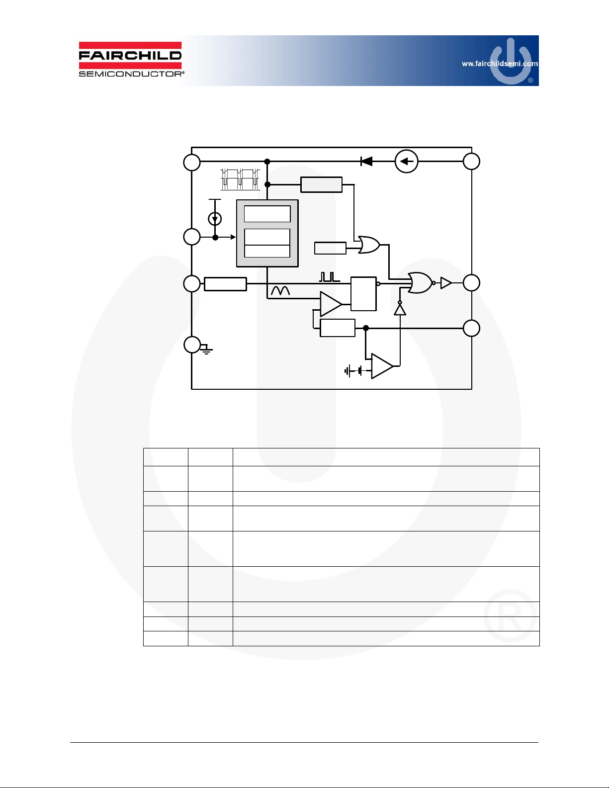
1.3. Internal Block Diagram
HV
VCC
3
VCC
ZCD
time
I
AD
ZCD
UVLO
JFET
8
ADIM
RT
GND
5
Oscillator
4
6
DAC
Soft-Start
Digital Block
Reference
TSD
+
LEB
Leading-Edge
Blanking
Q
R
S
AOCP
+
2.5V
OUT
2
1
CS
Figure 1. Block Diagram
Table 1. Pin Definitions
Pin Name Description
1 CS
2 OUT
3 VCC
4 RT
5 ADIM
6 GND
7 NC No Connection
8 HV
Current Sense. Limits output current, depending on the sensing resistor
voltage. The CS pin is also used to set the LED current regulation.
Output. Connects to the MOSFET gate.
Supply Voltage. Supply pin for stable IC operation; ZCD signal detection
used for accurate PFC function.
Resistor. Programmable operating frequency using an external resistor
connected to this PIN and the IC has fixed frequency when this pin is left
open or floating.
Analog Dimming. Connects to the internal current source and can change
the output current using an external resistor. If ADIM is not used, connect a
0.1µF bypass capacitor between ADIM and GND.
GROUND. Ground for the IC.
High Voltage. Connect to the high-voltage line and supply current to the IC
© 2012 Fairchild Semiconductor Corporation 4 FEB-L034_FL7701 • Rev. 1.0.0

2. General Specifications for Evaluation Board
All data for this table was measured at an ambient temperature of 25°C.
Table 2. Summary of Features and Performance
Description Symbol Value Comments
V
90V Minimum Input Voltage
IN.MIN
Input Voltage Range
AC Input Frequency
Output Voltage
Output Current
Output Power
(1)
(2)
Efficiency
Temperature
Initial Application
Notes:
1. The output current has I
in parallel with the LED. Ensure the capacitor voltage rating is high enough to withstand an
open-LED condition or use a Zener diode for protection.
2. The output power is not equal to the apparent power due to the slight phase shift between the
output voltage and current.
V
IN.NORMAL
V
f
f
V
OUT,MAX
V
OUT,NORMAL
V
I
OUT.NORMAL
CC deviation < ±4.5%
110V / 220V Normal Input Voltage
264V Maximum Input voltage
IN.MAX
47Hz Minimum Input Frequency
IN.MIN
64Hz Maximum Input Frequency
IN.MAX
41V Maximum Output Voltage
39V Normal Output Voltage
37V Minimum Output Voltage
OUT,MIN
470mA Normal Output Current
Line Input Voltage Change:
Output Power 18.3W
>83% At Full Load
T
< 63°C
FL7701
T
< 69°C
DM filter
T
FRD,ES3J
T
MOSFET
T
inductor
PCB Size
ripple. To reduce ripple current, use a large electrolytic capacitor
LEDPK
< 61°C
< 68°C
< 50°C
At full load (all at open-frame,
room temperature / still air)
18mm (width) x 295mm (length) x
90~264VAC
10mm (height)
L-Tube
© 2012 Fairchild Semiconductor Corporation 5 FEB-L034_FL7701 • Rev. 1.0.0

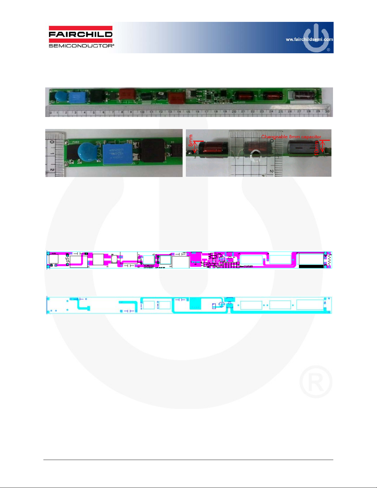
3. Photographs
Figure 3. Width: 18mm Figure 4. Height: 10mm (Include PCB)
Figure 2. Top View, Length: 295mm
4. Printed Circuit Board
Figure 5. Top Side (18mm x 295mm)
Figure 6. Bottom Side (18mm x 295mm)
© 2012 Fairchild Semiconductor Corporation 6 FEB-L034_FL7701 • Rev. 1.0.0

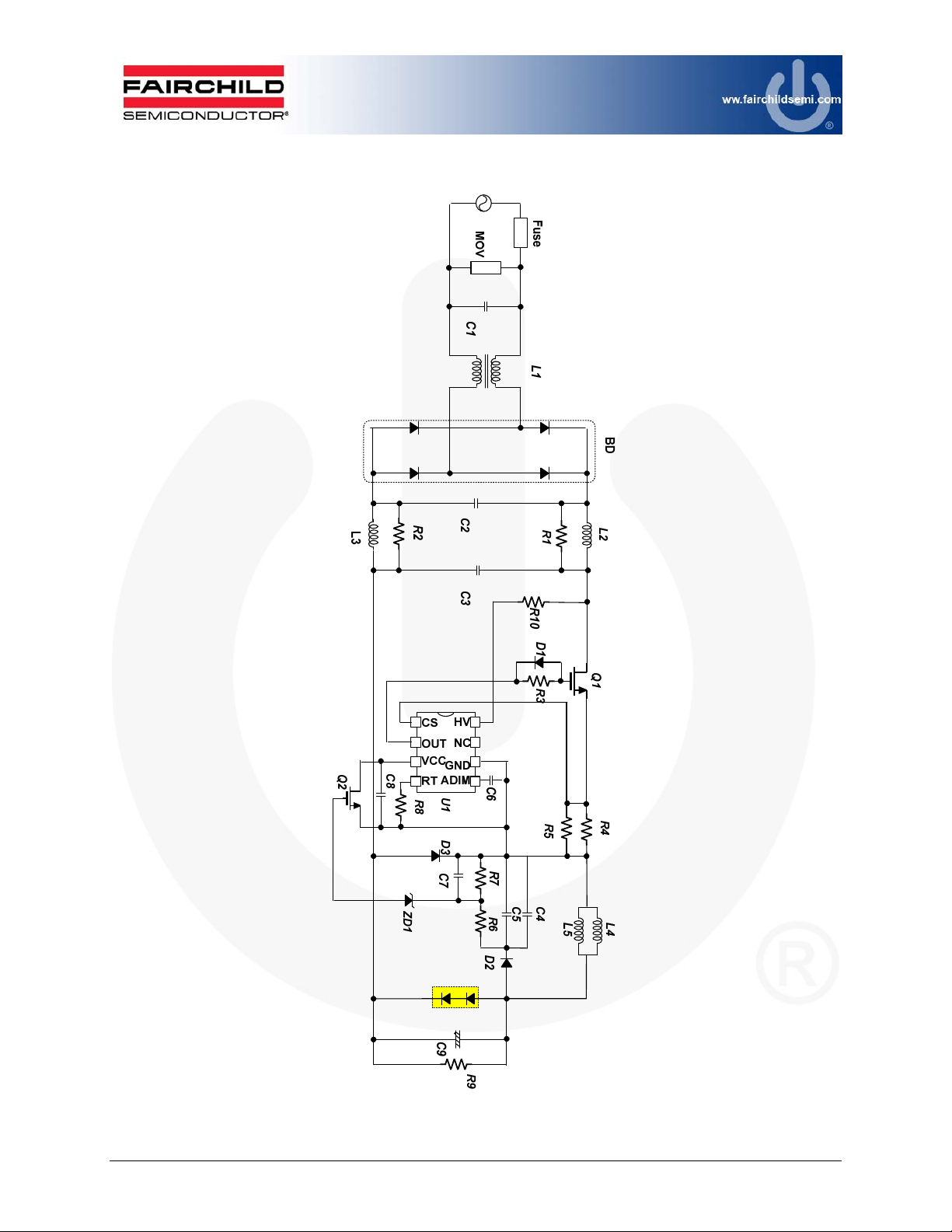
5. Schematic
Figure 7. Schematic
© 2012 Fairchild Semiconductor Corporation 7 FEB-L034_FL7701 • Rev. 1.0.0

6. Bill of Materials
Item
No.
1 U1 FL7701 1 Controller Fairchild Semiconductor
2 Fuse SS-5-1A 1 1A/250V Fuse Cooper Bussmann
3 MOV MOV-10D471K 1 VARISTOR 470V 10MM RADIAL Bourns Inc.
4 L1 LF-1480-253 1 Line Filter
5 L2, L3 RFB0810-472 2 4.7mH Inductor Coil Craft
6 L4, L5 PCH-45x-475 2 4.7mH Inductor Coil Craft
7 BD DF04S 1 400V / 1.5A, Bridge Rectifier Fairchild Semiconductor
8 D1 1N4148 1
9 D2 RS1M 1 1000V / 1A, Fast Rectifier F airchild Semiconductor
10 D3 ES3J 1 600V / 3A, Fast Rectifier Fairchild Semiconductor
11 ZD1 MMSZ5230B 1 4.7V / 0.5W Zener Diode Fairchild Semiconductor
12 Q1 FQD2N60 1 2A / 600V MOSFET Fairchil d Semiconductor
13 Q2 FQN1N50C 1 1A / 500V MOSFET Fairchild Semiconductor
14 C1
15 C2 MPE 630V104K 1
16 C3 MPE 400V334K 1
Part
Reference
Part Number Qty. Description Manufacturer
Sejin Telecom
(www.sejintel.com)
PCX2 335M MKP
100nF
100V / 200mA, Small Signal
Diode
1 100nF / 275VAC, X-Cap PILKOR
0.1µF / 630VAC, 10%,
Polypropylene
0.33µF / 400VAC, 10%,
Polypropylene
Fairchild Semiconductor
Sungho
Sungho
17 C4, C5 C1206C225K5PACTU 2
18 C6
19 C7 C1206C102K5PACTU 1
20 C8 C1206C105K5PACTU 1
21 C9 KMG 330µF / 63V 1 330µF/63V Electrolytic Capacitor SamYoung
22 R1, R2 RC1106JR-07151RL 2
23 R3 RC0805JR-07331RL 1
24 R4, R5 RC1106JR-070R9RL 2
25 R6 RC1106JR-07204RL 1
26 R7 RC1106JR-07153RL 1
27 R8 RC0805JR-07823RL 1
28 R9 10.0KBZTB-ND 1
29 R10 RC1106JR-07000RL 1
C0805C104K3RACTU
2.2µF / 50V SMD Capacitor 3216
1
0.1µF / 25V SMD Capacitor 2012
1nF / 50V SMD Capacitor 3216
1µF / 50V SMD Capacitor 3216
150Ω RES, SMD, 1/4W, 3216
330Ω RES, SMD, 1/8W, 2012
0.9Ω RES, SMD, 1/4W, 3216
200kΩ RES, SMD, 1/4W, 3216
15kΩ RES, SMD, 1/4W, 3216
82kΩ RES, SMD, 1/8W, 2012
10kΩ / 1W Resistor
0Ω RES, SMD, 1/4W, 3216
Kemet
Kemet
Kemet
Kemet
Yageo
Yageo
Yageo
Yageo
Yageo
Yageo
Yageo
Yageo
© 2012 Fairchild Semiconductor Corporation 8 FEB-L034_FL7701 • Rev. 1.0.0
 Loading...