User Guide for
FEB-L032 Evaluation Board
2.7W LED Ballast Using FLS0116
Featured Fairchild Product:
FLS0116
Direct questions or comments
about this evaluation board to:
“Worldwide Direct Support”
Fairchild Semiconductor.com
© 2012 Fairchild Semiconductor Corporation 1 FEB-L032_FLS0116 • Rev. 1.0.1

Table of Contents
1. Introduction ............................................................................................................................... 3
1.1. General Description ......................................................................................................... 3
1.2. Key Features .................................................................................................................... 3
1.3. Internal Block Diagram .................................................................................................... 4
2. General Specifications for Evaluation Board ........................................................................... 5
2.1. Photographs of Evaluation Board .................................................................................... 6
2.2. Printed Circuit Board ....................................................................................................... 7
2.3. Schematic ......................................................................................................................... 8
2.4. Bill Of Materials .............................................................................................................. 8
3. Performance of Evaluation Board ............................................................................................. 9
3.1. Typical Waveforms: Startup .......................................................................................... 10
3.2. Operating Frequency & Minimum Duty ........................................................................ 11
3.3. Typical Waveforms: Steady State .................................................................................. 12
3.4. Typical Operating Waveforms: Output Characteristics ................................................. 13
3.5. Typical Waveforms: Abnormal Mode (LED Open) ...................................................... 15
3.6. Typical Waveforms: Abnormal Mode (Inductor Short) ................................................ 16
3.7. System Efficiency .......................................................................................................... 17
3.8. Power Factor at Rated Load Condition .......................................................................... 18
3.9. Total Harmonic Distortion ............................................................................................. 19
3.10. Thermal Performance ..................................................................................................... 20
3.11. EMI Test Results............................................................................................................ 22
4. Revision History ..................................................................................................................... 24
© 2012 Fairchild Semiconductor Corporation 2 FEB-L032_FLS0116 • Rev. 1.0.1

This user guide supports the evaluation kit for the FLS0116. It should be used in
conjunction with the FLS0116 datasheet as well as Fairchild’s application notes and
technical support team. Please visit Fairchild’s website at www.fairchildsemi.com
1. Introduction
This document describes the proposed solution for an universal input, 2.7W LED ballast
using the FLS0116. The input voltage range is 90V
output with a constant current of 97mA at 28V
description of FLS0116, the power supply specification, schematic, bill of materials and
the typical operating characteristics.
1.1. General Description
The FLS0116 LED lamp driver is a simple IC with PFC function and integrated
switching MOSFET. The special “adopted digital” technique automatically detects input
voltage condition and sends an internal reference signal, resulting in high power factor
(PF). When AC input voltage is applied to the IC, PFC function is automatically enabled.
When DC input voltage is applied to the IC, PFC function is automatically disabled. The
FLS0116 does not require a bulk capacitor (electrolytic capacitor) for supply rail
stability, which can significantly improve LED reliability.
– 265V
RMS
. This document contains general
MAX
and there is one DC
RMS
.
1.2. Key Features
Built-in MOSFET (1A/550V)
Digitally Implemented Active PFC Function
(No Additional Circuit Necessary for High PF)
Built-in HV Supplying Circuit: Self Biasing
AOCP Function with Auto-Restart Mode
Built-in Over-Temperature Protection (OTP)
Cycle-by-Cycle Current Limit
Low Operating Current: 0.85mA (Typical)
Under-Voltage Lockout with 5V Hysteresis
Programmable Oscillation Frequency
Programmable LED Current
Analog Dimming Function
Soft-Start Function
Precise Internal Reference: ±3%
© 2012 Fairchild Semiconductor Corporation 3 FEB-L032_FLS0116 • Rev. 1.0.1

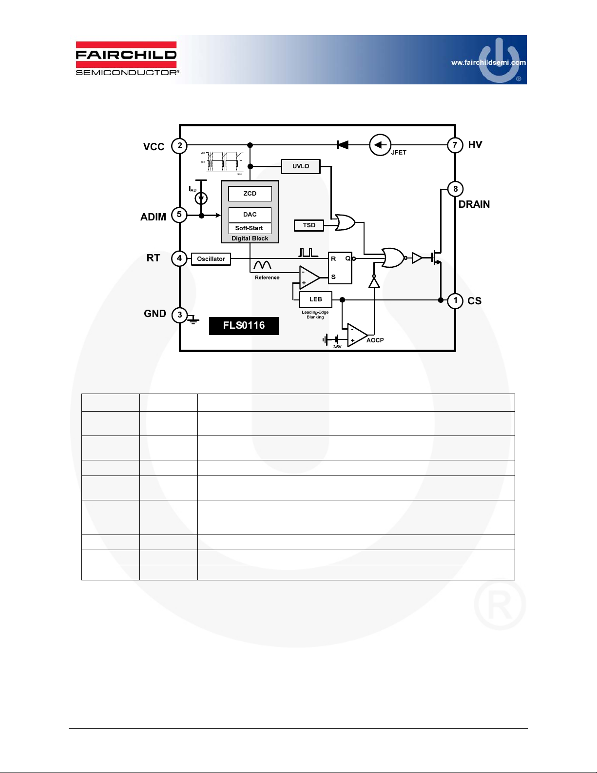
1.3. Internal Block Diagram
Figure 1. Internal Block Diagram
Pin No. Symbol Description
1 CS
2 VCC
3 GND
4 RT
5 ADIM
6 NC No Connection.
7 HV
8 DRAIN
Current Sense. Limits output current, depending on the sensing resistor
voltage. The CS pin is also used to set the LED current regulation.
VCC. Supply pin for stable IC operation ZCD signal detection used for accurate
PFC function.
GROUND. Ground for the IC.
RT. Programmable operating frequency using an external resistor. The IC has a
fixed frequency when this pin is open or floating.
Analog Dimming. Connects to the internal current source and can change the
output current using an external resistor. If ADIM is not used, connect a 0.1µF
bypass capacitor between ADIM and GND.
High Voltage. Connects to the high-voltage line and supplies current to the IC.
High Voltage. Internal switching FET drain pin.
© 2012 Fairchild Semiconductor Corporation 4 FEB-L032_FLS0116 • Rev. 1.0.1

2. General Specifications for Evaluation Board
All data for this table was measured at an ambient temperature of 25°C.
Table 1. Summary of Features and Performance
Description Symbol Value Comments
V
90V Minimum Input Voltage
IN.MIN
Input Voltage Range
AC Input Frequency
Output Voltage
Output Current
Output Power
(1)
(2)
Output Power 2.7W
Efficiency >78% At Full Load
Temperature
PCB Size
Initial Application LED Bulb
Notes:
1. The output current has I
in parallel with the LED. Ensure the capacitor voltage rating is high enough to withstand an
open-LED condition or use a Zener diode for protection.
2. The output power is not equal to the apparent power due to the slight phase shift between the
output voltage and current.
V
IN.NORMAL
V
Freq
Freq
V
OUT,MAX
V
OUT,NORMAL
V
I
OUT.NORMAL
CC Deviation < ±1.3%
T
T
T
FRD,UF4007
T
CS resistor
T
110V / 220V Normal Input Voltage
265V Maximum Input Voltage
IN.MAX
47Hz Minimum Input Frequency
IN.MIN
64Hz Maximum Input Frequency
IN.MAX
30V Maximum Output Voltage
28V Normal Output Voltage
26V Minimum Output Voltage
OUT,MIN
97mA Normal Output Current
Line Input Voltage Change:
90~265VAC
< 73°C
FLS0116
< 44°C
DM filter
< 47°C
At Full Load (all at open-frame, room
temperature / still air)
< 59°C
< 66°C
inductor
20mm (width) x 30mm (length )x
18mm (height)
ripple. To reduce ripple current, use a large electrolytic capacitor
LEDPK
© 2012 Fairchild Semiconductor Corporation 5 FEB-L032_FLS0116 • Rev. 1.0.1

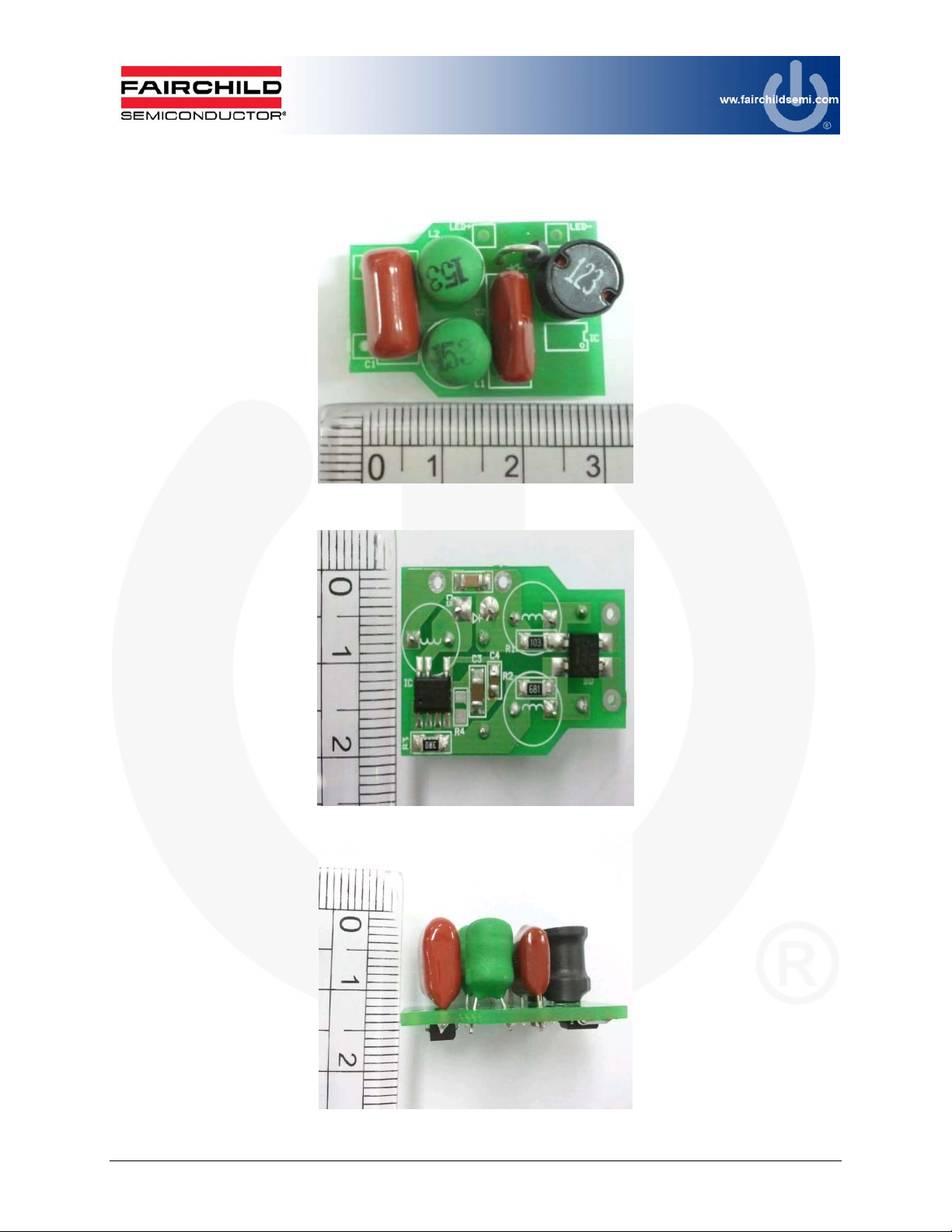
2.1. Photographs of Evaluation Board
Figure 2. Top View (20mm x 30mm)
Figure 3. Bottom View (20mm x 30mm)
Figure 4. Side View (18mm)
© 2012 Fairchild Semiconductor Corporation 6 FEB-L032_FLS0116 • Rev. 1.0.1

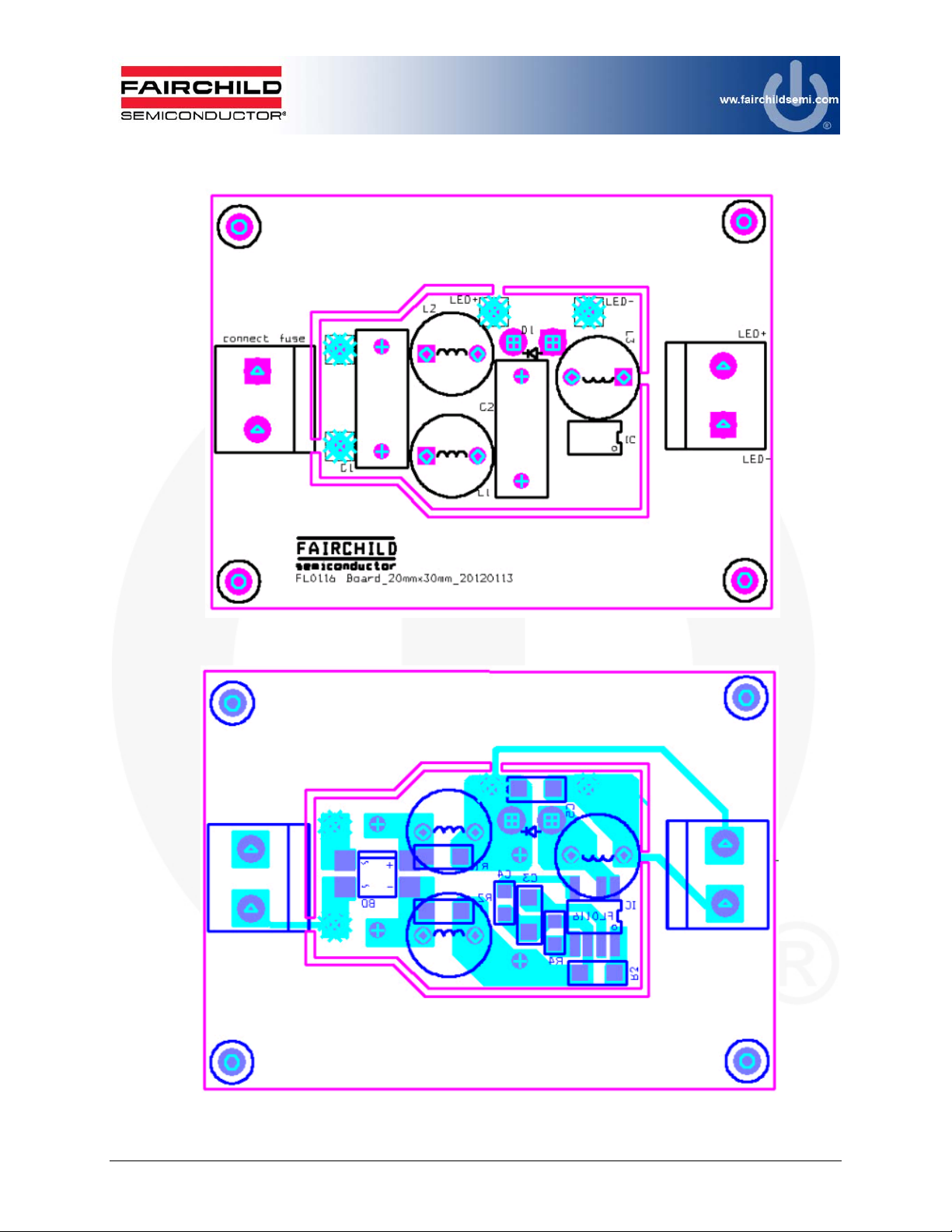
2.2. Printed Circuit Board
Figure 5. Top Side
Figure 6. Bottom Side
© 2012 Fairchild Semiconductor Corporation 7 FEB-L032_FLS0116 • Rev. 1.0.1

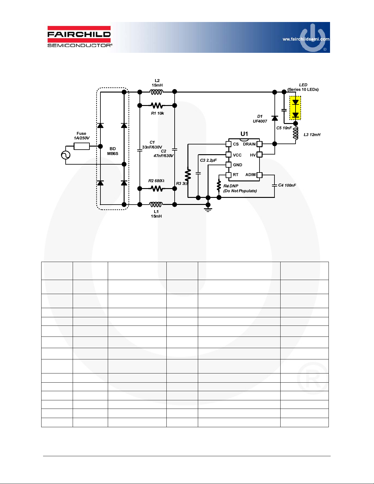
2.3. Schematic
Figure 7. Evaluation Board Schematic
2.4. Bill Of Materials
Item No.
1 U1 FLS0116M 1 Controller
2 BD MB6S 1 0.5A/600V, Bridge Diode
3 C1 MPE 630V333K 1 333/630VAC, Film Capacitor Sungho
4 C2 MPE 630V473K 1 473/630VAC, Film Capacitor Sungho
5 C3 C1206C225K3PACTU 1
6 C4
7 C5 C1206C103KDRACTU 1
8 D1 UF4007 1 1A/1000V, Ultra-Fast Recovery
9 L1,L2 R06153KT00 2 15mH, Filter Inductor Bosung
10 L3 RFB0810-123L 1 12mH, Inductor Coil Craft
11 R1 RC1206JR-07103RL 1 10kΩ, SMD Resistor 3216 Yageo
12 R2 RC1206JR-07680RL 1 680Ω, SMD Resistor 3216 Yageo
13 R3 RC1206JR-073RL 1 3Ω, SMD Resistor 3216 Yageo
- R4 - 0 Open
Part
Reference
Part Number Qty. Description Manufacturer
Fairchild
Semiconductor
Fairchild
Semiconductor
Kemet
Kemet
Kemet
Fairchild
Semiconductor
C0805C104K3RACTU
225/25V SMD Capacitor 3216
1
104/25V SMD Capacitor 2012
103/630V SMD Capacitor 3216
© 2012 Fairchild Semiconductor Corporation 8 FEB-L032_FLS0116 • Rev. 1.0.1
 Loading...