

Page 1

User Guide for
FEBFOD8012_RS485
Evaluation Board
Bi-Directional Logic Gate Optocoupler
Provides Proven and Reliable Isolation to
the RS485 Interface
Featured Fairchild Product:
FOD8012
Direct questions or comments
about this evaluation board to:
“Worldwide Direct Support”
Fairchild Semiconductor.com
© 2012 Fairchild Semiconductor Corporation FEBFOD8012_RS485 • Rev. 1.0.0
Page 2

Table of Contents
1. Introduction ............................................................................................................................... 3
1.1. Description ....................................................................................................................... 3
2. Photographs............................................................................................................................... 4
3. Printed Circuit Board ................................................................................................................ 4
3.1. Board Setup and Operation .............................................................................................. 5
3.2. Test Procedures and Conditions ....................................................................................... 5
4. Schematic .................................................................................................................................. 6
5. Scope Shots ............................................................................................................................... 7
6. Conclusion ................................................................................................................................ 8
7. Revision History ....................................................................................................................... 9
© 2012 Fairchild Semiconductor Corporation 2 FEBFOD8012_RS485 • Rev. 1.0.0
Page 3
This user guide supports the evaluation kit for the FOD8012. It should be used in
conjunction with the FOD8012 datasheet as well as Fairchild’s application notes and
technical support team. Please visit Fairchild’s website at www.fairchildsemi.com.
1. Introduction
The FOD8012 is an industry-first, full-duplex, bi-directional, logic-gate optocoupler with
high noise immunity as well as proven and reliable optical isolation. It is highly
integrated with two optically coupled channels arranged in a bi-directional configuration
illustrated in Figure 1. The FOD8012 is housed in a compact 8-pin small outline package.
Each optocoupler channel consists of a high-speed AIGaAs LED driven by a CMOS
buffer IC coupled to a CMOS detector IC.
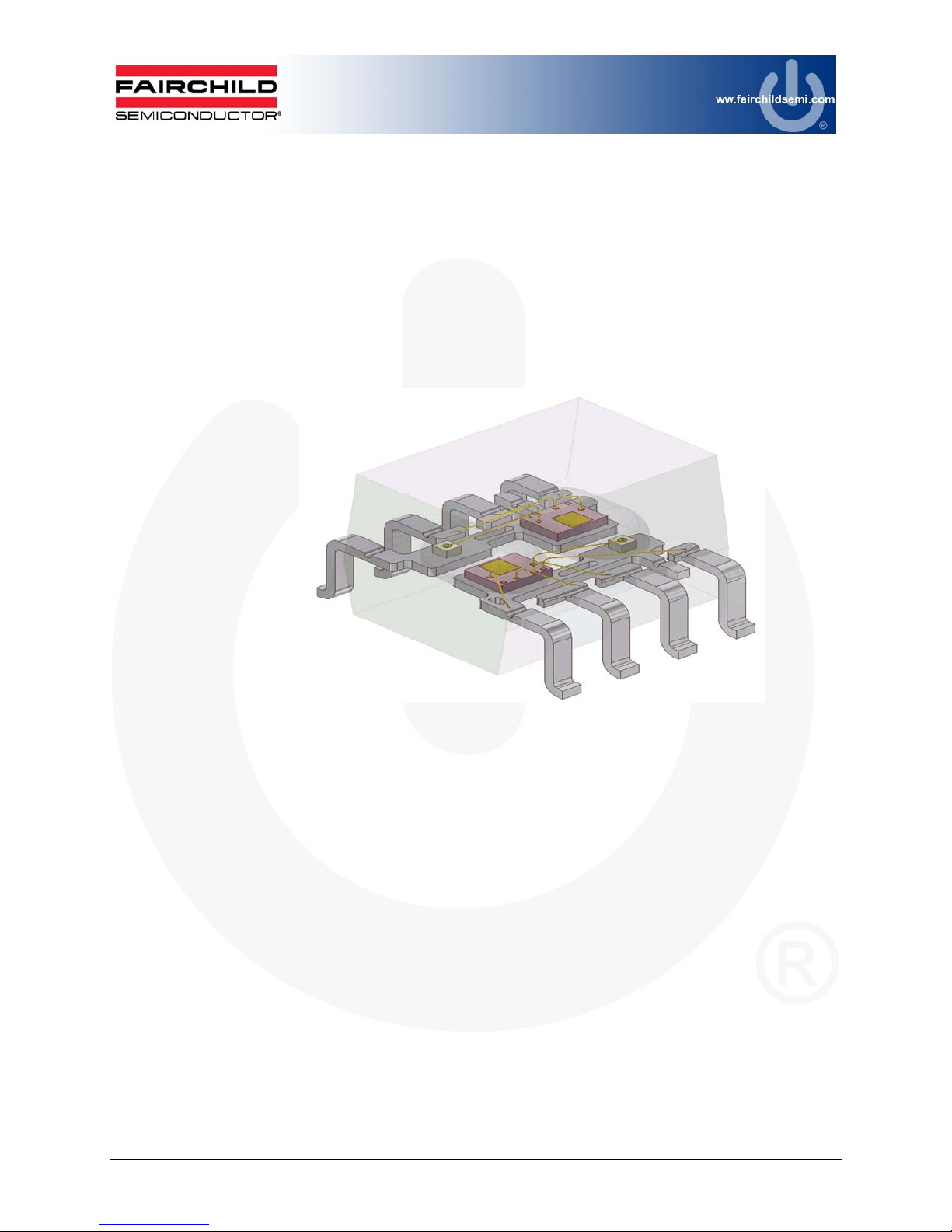
Figure 1. 3-Dimensional Illustration of the Internal Die Set of Fairchild’s Optoplanar®
1.1. Description
The FOD8012 supports isolated communication between systems of digital signals
without conducting ground loops or hazardous voltages. Unlike competitive devices,
which provide less than 0.1 mm optical isolation gap, the FOD8012 features a 0.4 mm
(minimum) optical isolation gap for proven, reliable isolation. The device also features a
fast switching speed, up to 15Mbit/sec, and uses Fairchild’s Optoplanar
technology and optimized IC design to achieve high Common Mode Rejection (CMR) of
20 kV/μs minimum, allowing the device to operate in noisy industrial environments.
Additionally, the FOD8012 offers an extended industrial temperature range of -40°C to
+110ºC and a 3.3 V or 5.0 V supply voltage to facilitate logic level translation. The
device’s high isolation voltage is certified by UL1577 and DIN_EN/IEC60747-5-2 for
increased reliability.
Package Construction
®
packaging
© 2012 Fairchild Semiconductor Corporation 3 FEBFOD8012_RS485 • Rev. 1.0.0
Page 4

2. Photographs
The evaluation board kit includes the FOD8012, a bi-directional logic-gate optocoupler
that isolates the driver input and receiver output of a half-duplex 3.3V RS485 transceiver.
In addition, a single-channel logic-gate optocoupler with open collector output,
FODM8061, isolates the driver-enable pin of the transceiver.
Figure 2. Photographs of the FEBFOD8012_RS485 Board
3. Printed Circuit Board
Figure 3. FEBFOD8012_RS485 Board Setup
© 2012 Fairchild Semiconductor Corporation 4 FEBFOD8012_RS485 • Rev. 1.0.0
Page 5

3.1. Board Setup and Operation
The FEBFOD8012_RS485 evaluation board enables users to make a quick and accurate
assessment of Fairchild’s FOD8012 in a bi-directional data transmission application. The
setup requires two power supply sources. V
with V
and VCC (J2) is on the other side of the isolation barrier, sharing the same
DD2
DD1
power supply source. A square wave is applied to one of the FOD8012 channels (VINB /
VOB), which in turn drives the RS485 transceiver. The resulting RS485 output is fed
back to the input of the other FOD8012 channel (VINA / VOA). This completes the bidirectional data transmission loop. Test points located at selected positions (as indicated
in Figure 3 and Figure 4) allow the user to probe the signals and measure the switching
characteristics of the device.
3.2. Test Procedures and Conditions
The steps below and Figure 3 describe the default setup of the FEBFOD8012_RS485
evaluation board.
1. Jumpers JP1 and JP2 are connected on the board by default. They connect the RS485
transceiver output to the resistive and capacitive loads: R4 (54 Ω), and C4 and C5
(each 100 pF), respectively. The user has the flexibility of connecting the RS485
driver output/receiver inputs to another load / signal source using the BNC (485+ and
485–) connectors and removing the jumpers (not covered in this document).
(J1) is on one side of the isolation barrier
2. With the power off, connect the power supplies to the board. They are set to
5.0 V (J1) or 3.3 V (J2), as specified on the board. Make sure that the supply voltages
do not exceed the absolute maximum rating of the devices, as this may damage
the devices.
3. Turn on the power supplies.
4. Apply a “HIGH” (5.0 V) to the BNC connector JR3 to enable the RS485 transceiver.
The user can synchronize the signal at JR3 with that at JR2 using another signal
source (e.g., using a dual-output signal generator). Application of a constant 5.0 V to
JR3 using a power supply is also sufficient.
5. Connect the output of the signal generator to the BNC connector (JR2). The signal
generator settings are: square wave = 1.25 MHz, duty cycle = 50%, amplitude =
5.0 V, output impedance = 50 Ω.
6. Enable the signal generator. The signal waveforms can be probed at various test
points, as shown in Figure 3:
TP1: VOA (RX) is the output voltage from channel-A of the FOD8012.
TP2: VINB (TX) is the input voltage to channel-B of the FOD8012. Signal from
the signal generator is applied here.
TP3: VINA is the input voltage to channel-A of the FOD8012. This signal is
supplied by the RS485 transceiver.
TP4: VOB is the output voltage from channel-B of the FOD8012, which in turn
drives the input of the RS485 transceiver.
TP5 & TP6: 485+ and 485- are the RS485 transceivers outputs.
TP7 to TP10: grounds.
© 2012 Fairchild Semiconductor Corporation 5 FEBFOD8012_RS485 • Rev. 1.0.0
Page 6

4. Schematic
The FEBFOD8012_RS485 board is designed for evaluation of the FOD8012 timing
sequence and AC test performance with an RS485 transceiver. It should be used in
conjunction with the product datasheet.
© 2012 Fairchild Semiconductor Corporation 6 FEBFOD8012_RS485 • Rev. 1.0.0
Figure 4. Evaluation Board Schematic
Page 7

5. Scope Shots
The scope shots in Figure 5 through Figure 7 illustrate normal operation of the
RS485 data transfer via the isolated channels of the FOD8012. Refer to Figure 4 for the
circuit schematic.
Figure 5. DRIVER_EN and VINB are Input Signals; FOD8012 Output Signal, VOB, Drives
RS485 Transceiver
Figure 6. FOD8012 Output Signal, VOB, Drives the RS485 Transceiver; Resulting RS485
Output Signals, V
and VB, are Single-Ended Output Signals; V
A
Output Signal
= Differential
(A-B)
© 2012 Fairchild Semiconductor Corporation 7 FEBFOD8012_RS485 • Rev. 1.0.0
Page 8

Figure 7. Output Signal from RS485 Transceiver Drives the Input, VINA, of FOD8012;
6. Conclusion
VOA is FOD8012 Output Signal
The FEBFOD8012_RS485 evaluation board allows the user to evaluate the performance
of the FOD8012 in a bi-directional data-transmission application with the RS485
transceiver. Measurement results clearly demonstrate the high-speed performance of
the FOD8012.
© 2012 Fairchild Semiconductor Corporation 8 FEBFOD8012_RS485 • Rev. 1.0.0
Page 9

7. Revision History
Rev. Date Description
1.0.0 August 2012 Initial Release
WARNING AND DISCLAIMER
Replace components on the Evaluation Board only with those parts shown on the parts list (or Bill of Materials) in the Users’ Guide. Contact an
authorized Fairchild representative with any questions.
This board is intended to be used by certified professionals, in a lab environment, following proper safety procedures. Use at your own risk. The
Evaluation board (or kit) is for demonstration purposes only and neit her the Board nor this User’s Guide constitute a sales contract or create any kind
of warranty, whether express or implied, as to the applications or products involved. Fairchild warrantees that its products meet Fairchild’s published
specifications, but does not guarantee that its products work in any specific application. Fairchild reserves the right to make changes without notice to
any products described herein to improve reliability, function, or design. Either the applicable sales contract signed by Fairchild and Buyer or, if no
contract exists, Fairchild’s standard Terms and Conditions on the back of Fairchild invoices, govern the terms of sale of the products described herein.
DISCLAIMER
FAIRCHILD SEMICONDUCTOR RESERVES THE RIGHT TO MAKE CHANGES WITHOUT FURTHER NOTICE TO ANY PRODUCTS HEREIN TO
IMPROVE RELIABILITY, FUNCTION, OR DESIGN. FAIRCHILD DOES NOT ASSUME ANY LIABILITY ARISING OUT OF THE APPLICATION OR
USE OF ANY PRODUCT OR CIRCUIT DESCRIBED HEREIN; NEITHER DOES IT CONVEY ANY LICENSE UNDER ITS PATENT RIGHTS, NOR
THE RIGHTS OF OTHERS.
LIFE SUPPORT POLICY
FAIRCHILD’S PRODUCTS ARE NOT AUTHORIZED FOR USE AS CRITICAL COMPONENTS IN LIFE SUPPORT DEVICES OR SYSTEMS
WITHOUT THE EXPRESS WRITTEN APPROVAL OF THE PRESIDENT OF FAIRCHILD SEMICONDUCTOR CORPORATION.
As used herein:
1. Life support devices or systems are devices or systems which, (a)
are intended for surgical implant into the body, or (b) support or
sustain life, or (c) whose failure to perform when properly used in
accordance with instructions for use provided in the labeling, can be
reasonably expected to result in significant injury to the user.
ANTI-COUNTERFEITING POLICY
Fairchild Semiconductor Corporation's Anti-Counterfeiting Policy. Fairchild's Anti-Counterfeiting Policy is also stated on our external website,
www.fairchildsemi.com, under Sales Support.
Counterfeiting of semiconductor parts is a growing problem in the industry. All manufacturers of semiconductor products are experiencing
counterfeiting of their parts. Customers who inadvertently purchase counterfeit parts experience many problems such as loss of brand reputation,
substandard performance, failed applications, and increased cost of production and manufacturing delays. Fairchild is taking strong measures to
protect ourselves and our customers from the proliferation of counterfeit parts. Fairchild strongly encourages customers to purchase Fairchild parts
either directly from Fairchild or from Authorized Fairchild Distributors who are listed by country on our web page cited above. Products customers buy
either from Fairchild directly or from Authorized Fairchild Distributors are genuine parts, have full traceability, meet Fairchild's quality standards for
handling and storage and provide access to Fairchild's full range of up-to-date technical and product information. Fairchild and our Authorized
Distributors will stand behind all warranties and will appropriately address any warranty issues that may arise. Fairchild will not provide any warranty
coverage or other assistance for parts bought from Unauthorized Sources. Fairchild is committed to combat this global problem and encourage our
customers to do their part in stopping this practice by buying direct or from authorized distributors.
EXPORT COMPLIANCE STATEMENT
These commodities, technology, or software were exported from the United States in accordance with the Export Administration Regulations for the
ultimate destination listed on the commercial invoice. Diversion contrary to U.S. law is prohibited.
U.S. origin products and products made with U.S. origin technology are subject to U.S Re-export laws. In the event of re-export, the user will be
responsible to ensure the appropriate U.S. export regulations are followed.
2. A critical component is any component of a life support device or
system whose failure to perform can be reasonably expected to
cause the failure of the life support device or system, or to affect its
safety or effectiveness.
© 2012 Fairchild Semiconductor Corporation 9 FEBFOD8012_RS485 • Rev. 1.0.0
Page 10

Mouser Electronics
Authorized Distributor
Click to View Pricing, Inventory, Delivery & Lifecycle Information:
Fairchild Semiconductor:
FEBFOD8012_RS485
 Loading...