

Page 1

Is Now Part of
To learn more about ON Semiconductor, please visit our website at
ON Semi conductor an d the ON Semico nductor logo a re trademar ks of Semicon ductor Comp onents Indus tries, L LC dba ON Semico nductor or it s subsidiari es in the United S tates and /or other coun tries. ON Se miconducto r owns the righ ts to a number
of patents, trademarks, copyrights, trade secrets, and other intellectual property. A listing of ON Semiconductor’s product/patent coverage may be accessed at www.onsemi.com/site/pdf/Patent-Marking.pdf. ON Semiconductor reserve s the right
to make changes without f urther noti ce to any produc ts herein. ON S emicon ductor makes no warran ty, representat ion or guar antee regar ding the suitability of its pro ducts for any partic ular purpose, n or does ON Semic onductor as sume any liabilit y
arisin g out of the applica tion or us e of any product o r circui t, and specific ally dis claims any and all lia bilit y, includin g witho ut limit ation sp ecial, c onsequential or incidental da mages . Buye r is responsib le for it s products and a pplica tions us ing ON
Semic onductor pr oducts, inc luding complia nce with all law s, regulati ons and safet y requirem ents or stan dards, rega rdless of an y support or ap plications in formation p rovided by ON S emiconduc tor. “Typical ” parameter s which may be pr ovided in ON
Semic onductor data s heet s and/or s pecificatio ns can and do vary in diff erent a pplica tions an d actual perf ormance may var y over time. All o perat ing parameter s, including “Typical s” must b e validated for e ach cus tomer ap plicat ion by customer’s
techni cal exper ts. ON Semic onductor do es not conve y any license un der its pate nt rights no r the rights o f others. ON S emiconduc tor produc ts are not des igned, inte nded, or autho rized for use a s a critical c omponent in lif e support s ystems or an y FDA
Clas s 3 medical devi ces or medica l devices wit h a same or similar c lassificat ion in a foreign j urisdictio n or any device s intended for im plantation in t he human body. Sho uld Buyer pur chase or use ON S emiconduct or products f or any such unint ended
or unaut horized appli cation, Buy er shall indemn ify and hold O N Semiconduc tor and its of ficers, e mployees , subsidiari es, affilia tes, and dis tributor s harmless ag ainst all claim s, costs , damages, an d expenses , and reason able attorn ey fees aris ing out
of, dire ctly or indire ctly, any claim o f personal inj ury or death as sociated w ith such unint ended or unauth orized use, e ven if such claim a lleges that ON S emiconduc tor was neglig ent regardin g the design or ma nufacture o f the part. ON S emiconduct or
is an Equa l Oppor tunity/Affirm ative Action E mployer. This li terature is s ubject to all applicable c opyright la ws and is no t for resale in any manner.
www.onsemi.com
Page 2

User Guide for
FEBFAN9611_S01U300A
Evaluation Board
FAN9611 300W Interleaved Dual-BCM,
Low-Profile, PFC Evaluation Board
Featured Fairchild Product:
FAN9611
Direct questions or comments
about this evaluation board to:
“Worldwide Direct Support”
Fairchild Semiconductor.com
© 2012 Fairchild Semiconductor Corporation 1 FEBFAN9611_S01U300A • Rev. 0.0.1
Page 3

Table of Contents
1. Overview of the Evaluation Board ............................................................................................. 3
2. Key Features ............................................................................................................................... 5
3. Specifications ............................................................................................................................. 6
4. Test Procedure ............................................................................................................................ 7
4.1. Safety Precautions .............................................................................................................7
5. Schematic ................................................................................................................................... 9
6. Boost Inductor Specification .................................................................................................... 10
7. Four-Layer PCB and Assembly Images ................................................................................... 11
8. Bill of Materials (BOM) ........................................................................................................... 14
9. Inrush Current Limiting ............................................................................................................ 16
10.Test Results ............................................................................................................................. 18
10.1.Startup .............................................................................................................................18
10.2.Steady State Operation ....................................................................................................20
10.3.Line Transient .................................................................................................................24
10.4.Load Transient ................................................................................................................25
10.5.Brownout Protection .......................................................................................................27
10.6.Phase Management .........................................................................................................28
10.7.Efficiency ........................................................................................................................30
10.8.Harmonic Distortion and Power Factor ..........................................................................32
10.9.EMI .................................................................................................................................33
11.References ............................................................................................................................... 34
12.Ordering Information .............................................................................................................. 34
13.Revision History ..................................................................................................................... 34
© 2012 Fairchild Semiconductor Corporation 2 FEBFAN9611_S01U300A • Rev. 0.0.1
Page 4

The following user guide supports the FAN9611 300W evaluation board for interleaved
boundary-conduction-mode power-factor-corrected supply. It should be used in
conjunction with the FAN9611 datasheet, Fairchild application note AN-6086 —Design
Considerations for Interleaved Boundary-Conduction Mode PFC Using FAN9611 /
FAN9612
and FAN9611/12 PFC Excel®-based Design Tool.
1. Overview of the Evaluation Board
The FAN9611 interleaved, dual Boundary-Conduction-Mode (BCM), Power-FactorCorrection (PFC) controllers operate two parallel-connected boost power trains 180º out
of phase. Interleaving extends the maximum practical power level of the control
technique from about 300W to greater than 800W. Unlike the Continuous Conduction
Mode (CCM) technique often used at higher power levels, BCM offers inherent zerocurrent switching of the boost diodes (no reverse-recovery losses), which permits the use
of less expensive diodes without sacrificing efficiency. Furthermore, the input and output
filters can be smaller due to ripple current cancellation between the power trains and
doubling of effective switching frequency.
The advanced line feed-forward with peak detection circuit minimizes the output voltage
variation during line transients. To guarantee stable operation with less switching loss at
light load, the maximum switching frequency is clamped at 525kHz. Synchronization is
maintained under all operating conditions.
Protection functions include output over-voltage, over-current, open-feedback, undervoltage lockout, brownout, and redundant latching over-voltage protection. FAN9611 is
available in a lead-free, 16-lead, Small-Outline Integrated-Circuit (SOIC) package.
This FAN9611 evaluation board uses a four-layer Printed Circuit Board (PCB) designed
for 300W (400V/0.75A) rated power. The maximum rated power is 350W and the
Maximum On-Time (MOT) power limit is set to 360W. The FEBFAN9611_S01U300A
is optimized to demonstrate all the FAN9611 efficiency and protection features in a lowprofile height form factor less than 18mm.
© 2012 Fairchild Semiconductor Corporation 3 FEBFAN9611_S01U300A • Rev. 0.0.1
Page 5
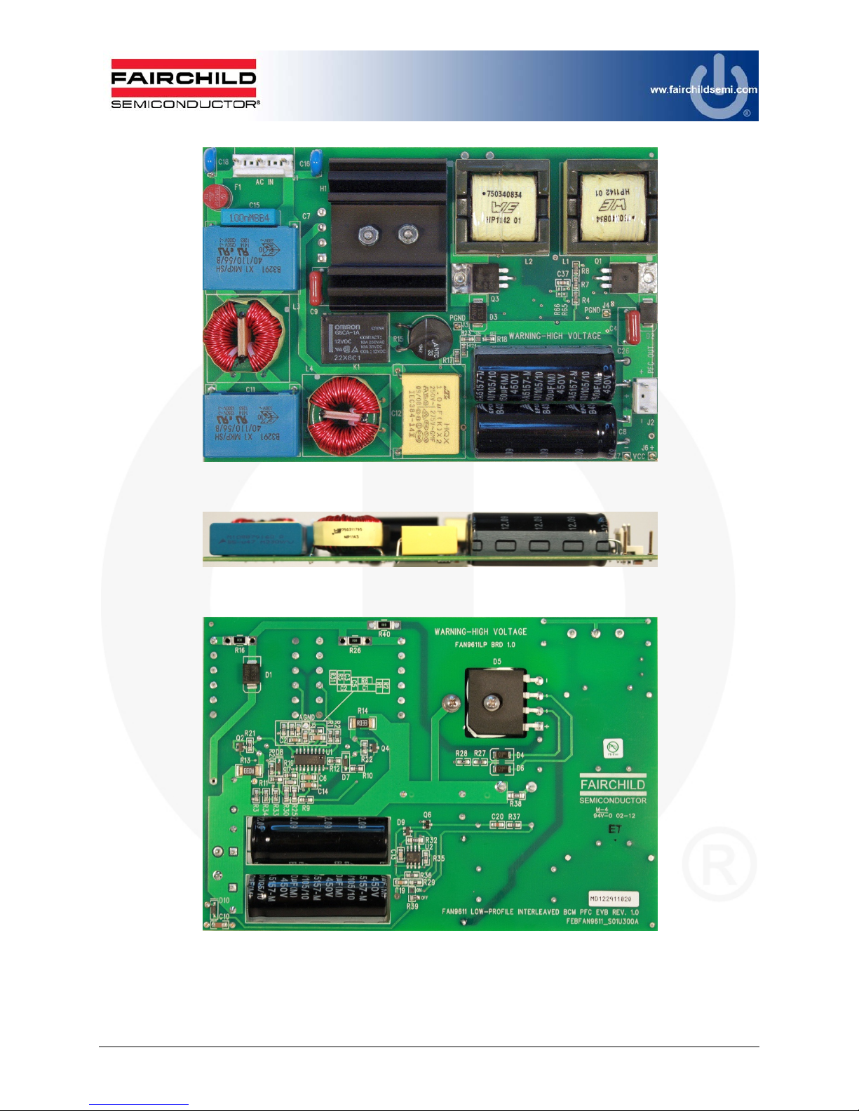
Figure 1. FEBFAN9611_S01U300A, Top View, 152mm x 105mm
Figure 2. FEBFAN9611_S01U300A, Side View (Low Profile), Cross Section=18mm
Figure 3. FEBFAN9611_S01U300A, Bottom View, 152mm x 105mm
© 2012 Fairchild Semiconductor Corporation 4 FEBFAN9611_S01U300A • Rev. 0.0.1
Page 6
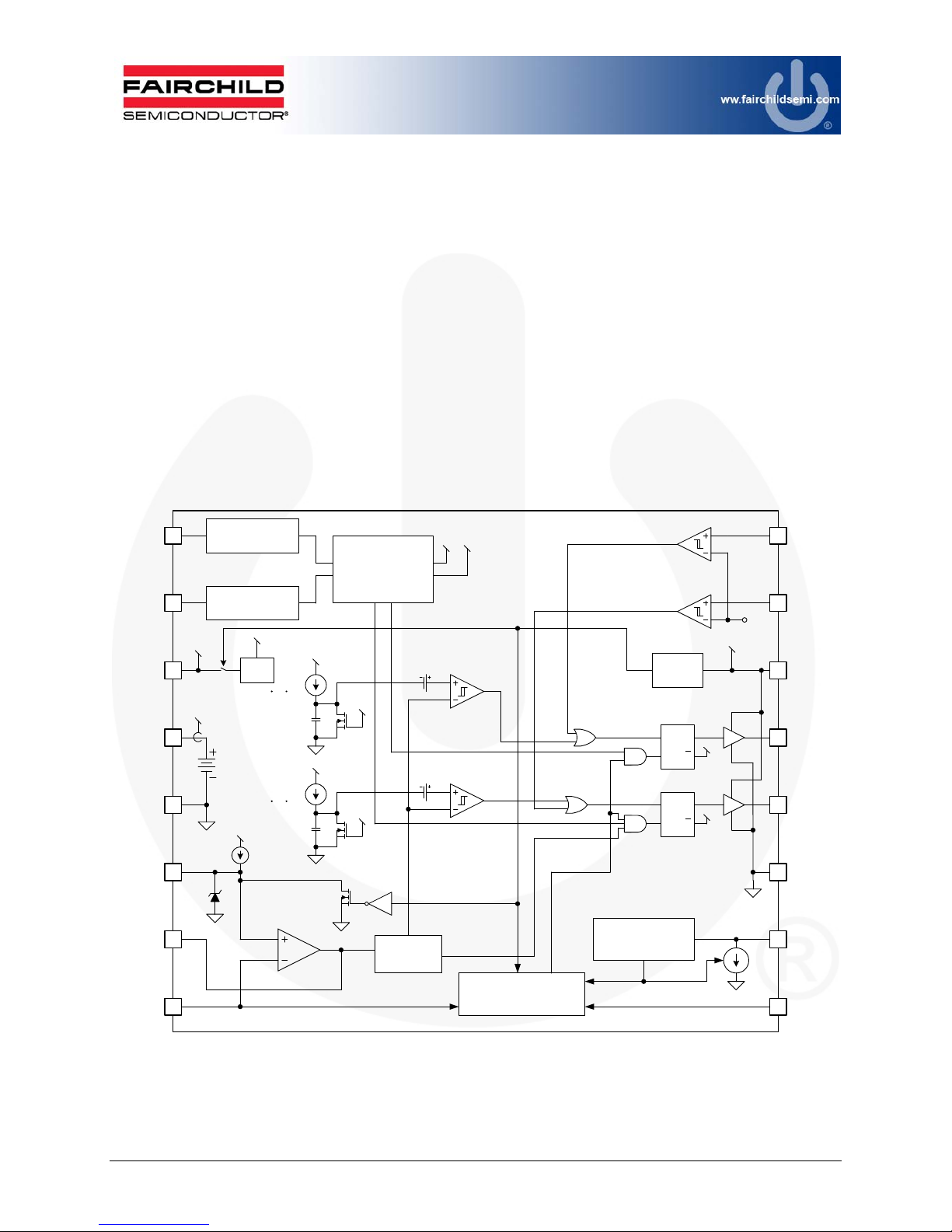
2. Key Features
180° Out-of-Phase Synchronization
Automatic Phase Disable at Light Load
1.8A Sink, 1.0A Source, High-Current Gate Drivers
Transconductance (g
Voltage-Mode Control with (V
Closed-Loop Soft-Start with Programmable Soft-Start Time for Reduced Overshoot
Minimum Restart Timer Frequency to Avoid Audible Noise
Maximum Switching Frequency Clamp
Brownout Protection with Soft Recovery
Non-Latching OVP on FB Pin and Second-Level Latching Protection on OVP Pin
Open-Feedback Protection
Over-Current and Power-Limit Protection for Each Phase
Low Startup Current: 80µA Typical
Works with DC input or 50Hz to 400Hz AC Input
) Error Amplifier for Reduced Overshoot
M
)2 Feed-Forward
IN
ZCD1
ZCD2
5VB
MOT
AGND
SS
COMP
FB
1
2
3
4
5
6
3V
7
8
VALLEY DETECTOR
VALLEY DETECTOR
5V
I
MOT
1.25V
REF
CHANNEL 1
CHANNEL 2
V
5V
BIAS
K1 VINI
K1 VINI
5V
5µA
16
0.2V
2µA
15
14
13
12
11
10
9
CS1
CS2
VDD
DRV1
DRV2
PGND
VIN
OVP
0.195V
0.195V
AB
PROTECTION LOGIC
(Open FB, Brownout Protec tion,
OVP, Latched OVP)
UVLO
S
S
INPUT VOLTAGE SENSE
(Input Voltage Squarer,
Input UVLO, Brownout)
V
DD
QQR
A
QQR
B
SYNCHRONIZATION
RESTART TIMERS
FREQUENCY CLAMPS
DD
5V
2
MOT
2
MOT
gm
A
5V
B
Phase
Management
Figure 4. Block Diagram
© 2012 Fairchild Semiconductor Corporation 5 FEBFAN9611_S01U300A • Rev. 0.0.1
Page 7
3. Specifications
This evaluation board has been designed and optimized for the conditions in Table 1.
Table 1. Electrical and Mechanical Requirements
Min. Typ. Max.
V
80V 120V 265V
IN_AC
P
P
V
V
V
OUT_PFC_RIPPLE
P
OUT_PFC(MOT LIMIT)
t
SOFT_START
t
ON_OVERSHOOT
>30%P
OUT
>30%P
OUT
90V
IN_AC(ON)
IN_AC(OFF)
f
50Hz 60Hz 65Hz
VIN_AC
V
395V 400V 405V
OUT_PFC
P
300W 350W
OUT_PFC
f
18kHz 300kHz
SW_P FC
t
20ms
HOLD_UP
250ms 300ms
_PFC_120V
OUT(TYP)
_PFC_230V
OUT(TYP)
PF
0.991
_120V
PF
0.980
_230V
Height 18mm
JC
80V
10V 11V
360W
10V
96% 96.5%
95% 98%
Mechanical and Thermal
60⁰C
The trip points for the built-in protections are set as below in the evaluation board.
The line UVLO (brownout protection) trip point is set at 80V
(10VAC hysteresis).
AC
The pulse-by-pulse current limit for each MOSFET is set at 6A.
The current-limit function can be observed by measuring the individual inductor current
waveforms while operating at 85V
power limit is set at ~120% of the rated output power. The power-limit function can be
observed while operating at >115V
operating in power limit, the output voltage drops and the COMP voltage is saturated, but
the AC line current remains sinusoidal. The phase-management function permits phase
shedding / adding ~18% of the nominal output power for high line (230V
can be increased by modifying the MOT resistor (R6) as described in Fairchild
Application Note AN-6086 —Design Considerations for Interleaved Boundary-
Conduction Mode PFC Using FAN9611 / FAN9612.
© 2012 Fairchild Semiconductor Corporation 6 FEBFAN9611_S01U300A • Rev. 0.0.1
and increasing the load to 360W. The maximum
AC
and increasing the load beyond 360W. When
AC
). This level
AC
Page 8
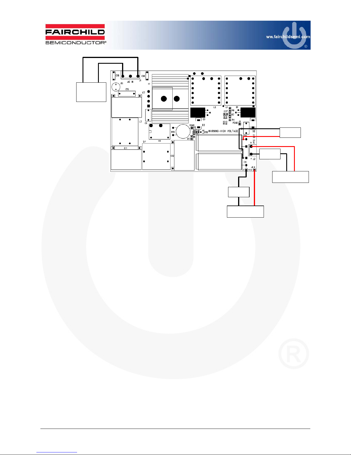
4. Test Procedure
Before applying power to the FEBFAN9611_S01U300A evaluation board; the DC bias
supply for V
should be connected to the board as shown in Figure 5.
Table 2. Specification Excerpt from FAN9611 Datasheet
Symbol Parameter Conditions Min. Typ. Max. Unit
Supply
I
STARTUP
IDD
I
DD_DYM
VON
V
OFF
V
HYS
4.1. Safety Precautions
The FEBFAN9611_S01U300A evaluation module produces lethal voltages and the bulk
output capacitors store significant charge. Please be extra careful when probing and
handling the module and observe a few precautions:
, AC voltage supply for line input, and DC electronic load for output
DD
Startup Supply Current VDD = VON – 0.2V
Operating Current Output Not Switching
Dynamic Operating Current fSW = 50kHz; C
UVLO Start Threshold VDD Increasing
UVLO Stop Threshold Voltage VDD Decreasing
UVLO Hysteresis V
ON
– V
OFF
80 110 µA
3.7 5.2 mA
= 2nF
LOAD
4 6 mA
9.5 10.0 10.5 V
7.0 7.5 8.0 V
2.5 V
Start with a clean working surface, clear of any conductive material.
Be careful while turning on the power switch to the AC source.
Never probe or move a probe on the DUT while the AC line voltage is present.
Ensure the output capacitors are discharged before disconnecting the test leads. One
way to do this is to remove the AC power with the DC output load still switched on.
The load then discharges the output capacitors and the module is safe to disconnect.
Power-On Procedure
1. Supply V
specification for V
2. Connect the AC voltage (90~265V
FAN9611 has brownout protection, any input voltage less than the designed
minimum AC line voltage triggers brownout protection. FEBFAN9611_S01U300A
does not start until the AC input voltage is greater than 90V
3. Change load current (0~0.75A) and check the operation
4. Verify the output voltage is regulating between 395V
for the control chip first. It should be higher than 10.5V (refer to the
DD
turn-on threshold voltage in Table 2).
DD
) to start the FAN9611 evaluation board. Since
AC
.
AC
DC<VOUT
<405VDC
© 2012 Fairchild Semiconductor Corporation 7 FEBFAN9611_S01U300A • Rev. 0.0.1
Page 9
AC Source
PF, THD, P
0-265V
AC
IN
DVM
Voltage
DVM
Current
Electronic Load
400V, 0-1A
DVM
Current
DC Bias Supply
0-12V
Figure 5. Recommended Test Set-Up
All efficiency data shown in this document was taken using the test set up shown in
Figure 5 with the output voltage being measured directly at the output bulk capacitors
(not through the output connector (J2)).
Power-Off Procedure
1. Make sure the electronic load is set to draw at least 100mA of constant DC current.
2. Disconnect (shut down) AC line voltage source.
3. Disconnect (shut down) 12V DC bias power supply.
4. Disconnect (shut down) DC electronic load last to ensure that the output capacitors
are fully discharged before handling the evaluation module.
© 2012 Fairchild Semiconductor Corporation 8 FEBFAN9611_S01U300A • Rev. 0.0.1
Page 10
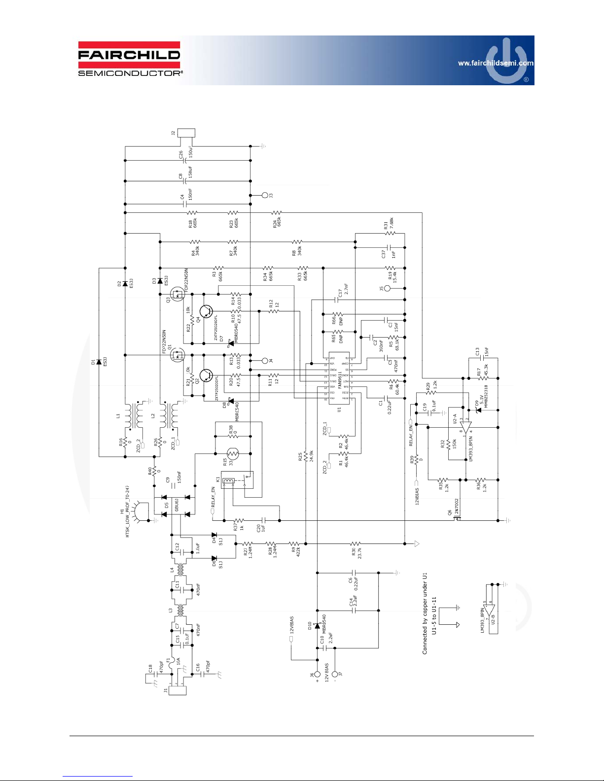
5. Schematic
Figure 6. FEBFAN9611_S01U300A 300W Evaluation Board Schematic
© 2012 Fairchild Semiconductor Corporation 9 FEBFAN9611_S01U300A • Rev. 0.0.1
Page 11
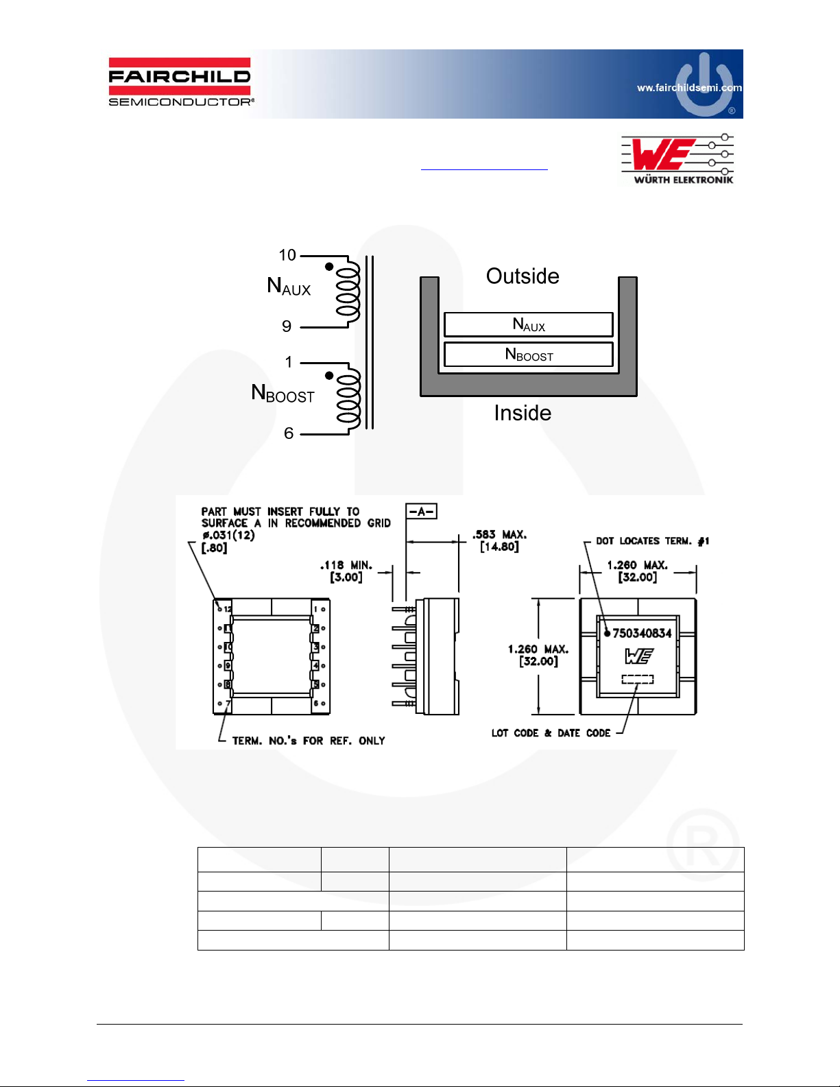
6. Boost Inductor Specification
750340834 from Wurth Electronics (www.we-online.com)
Core: EFD30 (A
=69mm2)
e
Bobbin: EFD30
Inductance : 270H
Figure 7. Boost Inductor (L1, L2) in the Evaluation Board
Figure 8. Wurth 750340834 Mechanical Drawing
Table 3. Inductor Turns Specifications
Pin Turns Wire
N
1 6 69 (3 Layers) 30xAWG#38 Litz
BOOST
Insulation Tape
N
10 9 7 AWG#28
AUX
Insulation Tape
© 2012 Fairchild Semiconductor Corporation 10 FEBFAN9611_S01U300A • Rev. 0.0.1
Page 12

7. Four-Layer PCB and Assembly Images
Figure 9. Layer 1 – Top Layer
© 2012 Fairchild Semiconductor Corporation 11 FEBFAN9611_S01U300A • Rev. 0.0.1
Figure 10. Layer 2 – Internal Layer
Page 13

Figure 11. Layer 3 – Internal Layer
© 2012 Fairchild Semiconductor Corporation 12 FEBFAN9611_S01U300A • Rev. 0.0.1
Figure 12. Layer 4 – Bottom Layer
Page 14

Figure 13. Top Assembly
© 2012 Fairchild Semiconductor Corporation 13 FEBFAN9611_S01U300A • Rev. 0.0.1
Figure 14. Bottom Assembly
Page 15

8. Bill of Materials (BOM)
Item Qty. Reference Part Number Value Description Manufacturer Package
1 2 C1, C6
2 1 C2
3 2 C3, C13
4 2 C4, C9 ECW-F2W154JAQ 150nF Cap, 450V, 5%, Polypropylene Panasonic Thru-Hole
5 1 C5
6 2 C7, C11 B32914A3474 470nF
7 2 C8, C26 B43041A5157M 150µF Cap, Alum, Elect. EPCOS Thru-Hole
8 2 C10, C14
9 1 C12 B32914A3105K 1µF
10 1 C15 PHE840MB6100MB05R17 0.1µF
11 2 C16, C18 CS85-B2GA471KYNS 470pF
12 1 C17
13 1 C19
14 1 C20 1µF CAP, SMD, Ceramic,50V, X5R STD 805
15 1 C37
16 3 D1-3 ES3J
17 2 D4, D6 S1J
18 1 D5 GBU6J
19 3 D7-8, D10 MBR0540
20 1 D9 MMBZ5231B 5.1V Diode, Zener, 5V, 350mW
21 1 F1 37421000410 10A
22 1 H1 7-345-2PP-BA Heatsink, Low Profile, T0-247 CTS Thru-Hole
23 1 J1 1-1318301-3 Header, 3 Pin, 0.312 Spacing TE Connectivity Thru-Hole
24 1 J2 1-1123724-2 Header, 2 Pin, 0.312 Spacing TYCO Thru-Hole
25 5 J3-7 3103-2-00-21-00-00-08-0 Test pin, Gold, 40mil, Mill-Max Thru-Hole
26 1 K1 G5CA-1A DC12
27 2 L1-2 750340834/NP1138-01 280µH Inductor, Coupled Wurth Thru-Hole
28 2 L3-4 750311795 9mH Common Mode Choke, 9mH Wurth Thru-Hole
29 2 Q1, Q3 FDP22N50N
0.22µF
390nF
15nF
470nF
2.2µF
2.7nF
0.1µF
1nF
CAP, SMD, Ceramic, 25V,
CAP, SMD, Ceramic, 25V,
CAP, SMD, Ceramic, 25V,
CAP, SMD, Ceramic, 25V,
CAP, SMD, Ceramic, 25V,
Cap, Ceramic, 250V
CAP, SMD, Ceramic, 25V,
CAP, SMD, Ceramic, 25V,
CAP, SMD, Ceramic, 25V,
Diode, 600V, 3A, Ultra-Fast
Diode, General Purpose, 1A,
Diode, Bridge, 6A, 1000V
Diode, Schottky,40V, 500mA
Fuse, 374 Series, 5.08mm
RELAY PWR SPST-NO 10A
MOSFET, NCH, UniFET,
X7R
X7R
X7R
X7R
Cap, 330VAC, 10%,
Polypropylene
X7R
Cap, 330V
Polypropylene
Cap, X Type, 10%,
Polypropylene
Y5P,
X7R
X7R
X7R
Recovery
600V
Spacing
12VDC PCB
500V, 11.5A, 0.18
, 10%,
AC
STD 1206
STD 805
STD 805
STD 805
EPCOS Thru-Hole
STD 1206
Epcos Thru-Hole
KEMET Thru-Hole
, 10%,
AC
TDK Corporation Thru-Hole
STD 805
STD 805
STD 805
Fairchild
Semiconductor
Fairchild
Semiconductor
Fairchild
Semiconductor
Fairchild
Semiconductor
Fairchild
Semiconductor
Littlefuse Radial
Omeron
Electronics, Inc.
Fairchild
Semiconductor
Continued on the following page…
SMC
SMA
Thru-Hole
SOD-123
SOT-23
Thru-Hole
TO-220
© 2012 Fairchild Semiconductor Corporation 14 FEBFAN9611_S01U300A • Rev. 0.0.1
Page 16

Item Qty. Reference Part Number Value Description Manufacturer Package
30 2 Q2, Q4 ZXTP25020DFL Transistor, PNP, 20V, 1.5A Zetex SOT-23
31 1 Q6 2N7002 MOSFET, NCH, 60V, 300mA Philips SOT-23
32 2 R1-2 46.4k RES, SMD, 1/8W STD 805
33 6
34 3 R4, R7-8 340k RES, SMD, 1/8W STD 805
35 1 R5 68.1k RES, SMD, 1/8W STD 805
36 1 R6 60.4k RES, SMD, 1/8W STD 805
37 1 R9 422k RES, SMD, 1/8W STD 805
38 2 R10, R20 47.5 RES, SMD, 1/8W STD 805
39 2 R11-12 12 RES, SMD, 1/8W STD 805
40 2 R13-14 0.033 RES, SMD, 1W STD 2512
41 1 R15 B57237S0330M000 33 Thermistor Epcos Inc. Thru-Hole
42 3
43 1 R17 45.3k RES, SMD, 1/8W STD 805
44 1 R19 15.4k RES, SMD, 1/8W STD 805
45 2 R21-22 10k RES, SMD, 1/8W STD 805
46 1 R25 24.9k RES, SMD, 1/4W STD 1206
47 2 R27-28 1.24M RES, SMD, 1/8W STD 805
48 3 R29, R35-36 1.2k RES, SMD, 1/8W STD 805
49 1 R30 23.7k RES, SMD, 1/4W STD 1206
50 1 R31 7.68k RES, SMD, 1/8W STD 805
51 1 R32 150k RES, SMD, 1/4W STD 1206
52 1 R37 1k RES, SMD, 1/8W STD 805
53 1 R38 0 RES, SMD, 1/4W STD 1206
54 1 R39 0 RES, SMD, 1/8W STD 805
55 2 R65-66 DNP RES, SMD, 1/10W STD 603
56 1 U1 FAN9611
57 1 U2 LM393M
58 2 SC1, SC2 PMSSS 440 0050 PH
59 2 W1, W2 INT LWZ 004
60 2 N1, N2 HNZ440 NUT HEX 4-40 ZINC PLATED STD Hardware
61 1 PWB
Notes:
1. DNP = Do Not Populate
2. STD = Standard Components
R3, R18,
R23-24 R33-
34
R16, R26,
R40
665k RES, SMD, 1/8W STD 805
0 RES, SMD, 1/2W STD 2010
Interleaved, Dual, BMC, PFC
Dual, Differential Comparator
SCREW MACHINE PHIL 4-
WASHER LOCK INT TOOTH
4 Layer, FR4, FAN9611 LOW-
PROFILE PWB - REV. 1.0
Controller
40X1/2 SS
#4 ZINC
Fairchild
Semiconductor
Fairchild
Semiconductor
STD Hardware
STD Hardware
Fairchild
Semiconductor
SOIC-16
SOIC-8
PCB
© 2012 Fairchild Semiconductor Corporation 15 FEBFAN9611_S01U300A • Rev. 0.0.1
Page 17

9. Inrush Current Limiting
The evaluation board includes an inrush current limiting circuit comprised of the highlighted
components shown in
Figure 15.
Since the inrush current limiting circuit has a negative impact on light-load efficiency and may not
be required by all offline applications, the evaluation board is configured with the inrush circuit
fully populated, but disabled, as shown in Figure 15. R18 and R39 are installed on the PCB;
purposely electrically open. To enable and test the inrush current limiting circuit, rotate R18 and
R39 to complete the proper series connection shown in the schematic. Remove R38 to allow the
33Ω NTC thermistor (R15) to limit the inrush current during startup. Input current measurements
can be made by removing the R16, 0Ω jumper and installing a loop of wire connected to the holes
provided within the R16 PCB pad locations. A current probe can then be connected to the wire
loop. The effectiveness of the inrush current limiting function is shown below in Figure 16.
© 2012 Fairchild Semiconductor Corporation 16 FEBFAN9611_S01U300A • Rev. 0.0.1
Figure 15. Inrush Current Limiting Circuit
Page 18

AC Input Current
(Inrush Enabled)
AC Input Current
(Inrush Disabled)
AC Input Peak
Current (Zoom)
(Inrush Disabled)
33 NTC
M2: AC Line Current (5A/div), CH3: AC Line Current (5A/div), Time (50ms/div)
Figure 16. Full-Load Startup at 115V
AC
Table 4. Inrush Current Limiting Circuit Effectiveness Comparison
Input Line
Voltage
VIN=115V
VIN=230V
Output
Power
300W 22.50A
AC
300W 26.9A
AC
Peak Line Current
(Inrush Circuit Disabled)
Peak Line Current
(Inrush Circuit Enabled)
8.45APK 62.40%
PK
11.5APK 57.3%
PK
% Inrush
Current
Reduction
© 2012 Fairchild Semiconductor Corporation 17 FEBFAN9611_S01U300A • Rev. 0.0.1
Page 19

10. Test Results
10.1. Startup
Figure 17 and Figure 18 show the startup operation at 115VAC line voltage for no-load
and full-load condition, respectively. Due to the closed-loop soft-start, almost no
overshoot is observed for no-load startup and full-load startup.
DRV1
COMP
V
OUT
Line
Current
CH1: Gate Drive 1 Voltage (20V/div), CH2: COMP Voltage (2V/div),
CH3: Output Voltage (200V/div), CH4: Line Current (5A/div), Time (100ms/div)
Figure 17. No-Load Startup at 115V
AC
DRV1
COMP
V
OUT
Line
Current
CH1: Gate Drive 1 Voltage (20V/div), CH2: COMP Voltage (2V/div),
CH3: Output Voltage (200V/div), CH4: Line Current (5A/div), Time (200ms/div)
Figure 18. Full-Load Startup at 115V
AC
© 2012 Fairchild Semiconductor Corporation 18 FEBFAN9611_S01U300A • Rev. 0.0.1
Page 20

Figure 19 and Figure 20 show the startup operation at 230V
line voltage for no-load
AC
and full-load conditions, respectively. Due to the closed-loop soft-start, almost no
overshoot is observed for no-load startup and full-load startup.
DRV1
COMP
V
OUT
Line
Current
CH1: Gate Drive 1 Voltage (20V/div), CH2: COMP Voltage (2V/div),
CH3: Output Voltage (200V/div), CH4: Line Current (10A/div), Time (100ms/div)
Figure 19. No-Load Startup at 230VAC
DRV1
COMP
V
Line
Current
OUT
CH1: Gate Drive 1 Voltage (20V/div), CH2: COMP Voltage (2V/div),
CH3: Output Voltage (200V/div), CH4: Line Current (10A/div), Time (100ms/div)
Figure 20. Full-Load Startup at 230V
AC
© 2012 Fairchild Semiconductor Corporation 19 FEBFAN9611_S01U300A • Rev. 0.0.1
Page 21

10.2. Steady-State Operation
Figure 21 and Figure 22 show the two inductor currents and the sum of the two inductor
currents operating at full load for 90V
inductor currents has relatively small ripple due to the ripple cancellation of interleaving.
IL2
I
L1
I
+ IL2
L1
and 230VAC line voltage. The sum of the
AC
CH3: Inductor L2 Current (5A/div), CH4: Inductor L1 Current (5A/div),
CH2: Sum of Two Inductor Currents (5A/div), Time (2ms/div, zoom to 10s/div)
Figure 21. Zoom of Inductor Current Waveforms at Full-Load and 90V
AC
IL2
I
L1
I
+ IL2
L1
CH3: Inductor L1 Current (2A/div), CH4: Inductor L2 Current (2A/div),
CH2: Sum of Two Inductor Current (2A/div), Time (2ms/div)
Figure 22. Zoom of Inductor Current Waveforms at Full-Load and 230V
AC
© 2012 Fairchild Semiconductor Corporation 20 FEBFAN9611_S01U300A • Rev. 0.0.1
Page 22

V
DS(Q3)
DRV1
ZCD1
I
L2
CH1: DRV1 (20V/div), CH2: VDS(Q3) (100V/div)
CH3: ZCD1 (1V/div), CH4: Inductor L2 Current (5A/div)
Figure 23. Zero Valley Switching at Full Load, 115V
AC
V
DS(Q3)
DRV1
ZCD1
IL2
Figure 24. Zero Valley Switching at Full Load, 230V
CH1: DRV1 (20V/div), CH2: VDS(Q3) (100V/div)
CH3: ZCD1 (1V/div), CH4: Inductor L2 Current (5A/div)
AC
© 2012 Fairchild Semiconductor Corporation 21 FEBFAN9611_S01U300A • Rev. 0.0.1
Page 23

V
DS(Q3)
I
L2
DRV1
CH1: DRV1 (20V/div), CH2: VDS(Q3) (100V/div)
CH4: Inductor L2 Current (5A/div)
Figure 25. Zoom of Valley Switching at Full Load, 230V
AC
CS1
CS2
IL2
I
L1
Figure 26. Current-Sense Waveforms at Full Load, 90VAC
CH1: FAN9611, Pin 16 (100mV/div), CH2: FAN9611, Pin 15 (100mV/div)
CH3: Inductor L2 Current (5A/div), CH4: Inductor L1 Current (5A/div)
© 2012 Fairchild Semiconductor Corporation 22 FEBFAN9611_S01U300A • Rev. 0.0.1
Page 24

IL1
I
L2
CH1: Inductor L1 Current (2A/div), CH2: Inductor L2 Current (2A/div)
Figure 27. Inductor Current Waveforms at 360W, 85V
, Over-Current Operation
AC
IL1
IL2
Line
Current
V
OUT
CH1: Inductor L1 Current (5A/div), CH2: Inductor L2 Current (5A/div)
CH3: Output Voltage (100V/div), CH4: Line Current (5A/div), Time (20ms/div)
Figure 28. MOT Power Limit, 0.5A to 1.3A Load Transient, 115VAC
© 2012 Fairchild Semiconductor Corporation 23 FEBFAN9611_S01U300A • Rev. 0.0.1
Page 25

10.3. Line Transient
V
V
Figure 29 and Figure 30 show the line transient operation and minimal effect on output
voltage due to the line feed-forward function. When the line voltage changes from
230V
observed. When the line voltage changes from 115V
nominal output voltage) voltage overshoot is observed.
to 115VAC, about 20V (5% of nominal output voltage) voltage undershoot is
AC
Rectified
Line
Voltage
OUT
COMP
Line
Current
to 230VAC, about 6V (1.5% of
AC
CH1: Rectified Line Voltage (200V/div), CH2: Output Voltage (20V/div, AC),
CH3: COMP Voltage (2V/div), CH4: Line Current (5A/div), Time (50ms/div)
Figure 29. Line Transient Response at Full-Load Condition (230VAC 115VAC)
Rectified
Line
Voltage
OUT
COMP
Line
Current
CH1: Rectified Line Voltage (200V/div), CH2: Output Voltage (10V/div, AC),
CH3: COMP Voltage (2V/div), CH4: Line Current (5A/div), Time (50ms/div)
Figure 30. Line Transient Response at Full-Load Condition (115V
230VAC)
AC
© 2012 Fairchild Semiconductor Corporation 24 FEBFAN9611_S01U300A • Rev. 0.0.1
Page 26

10.4. Load Transient
V
V
Figure 31 and Figure 32 show the load-transient operation. When the output load changes
from 100% to 0%, 20V (5% of nominal output voltage) voltage overshoot is observed.
When the output load changes from 0% to 100%, 34V (8.5% of nominal output voltage)
voltage undershoot is observed.
Rectified
Line
Voltage
OUT
COMP
Line
Current
CH1: Rectified Line Voltage (100V/div), CH2: Output Voltage (20V/div, AC),
CH3: COMP Voltage (2V/div), CH4: Line Current (5A/div), Time (50ms/div)
Figure 31. Load Transient Response at 115VAC (Full Load No Load)
Rectified
Line
Voltage
OUT
COMP
Line
Current
Figure 32. Load Transient Response at 115V
© 2012 Fairchild Semiconductor Corporation 25 FEBFAN9611_S01U300A • Rev. 0.0.1
CH1: Rectified Line Voltage (100V/div), CH2: Output Voltage (20V/div, AC),
CH3: COMP Voltage (2V/div), CH4: Line Current (5A/div), Time (50ms/div)
(No Load Full Load)
AC
Page 27

V
V
Rectified
Line
Voltage
OUT
COMP
Line
Current
CH1: Rectified Line Voltage (100V/div), CH2: Output Voltage (20V/div, AC),
CH3: COMP Voltage (5V/div), CH4: Line Current (5A/div), Time (50ms/div)
Figure 33. Load Transient Response at 230VAC (Full Load No Load)
Rectified
Line
Voltage
OUT
COMP
Line
Current
CH1: Rectified Line Voltage (100V/div), CH2: Output Voltage (20V/div, AC),
CH3: COMP Voltage (5V/div), CH4: Line Current (5A/div), Time (50ms/div)
Figure 34. Load Transient Response at 230V
(No Load Full Load)
AC
© 2012 Fairchild Semiconductor Corporation 26 FEBFAN9611_S01U300A • Rev. 0.0.1
Page 28

10.5. Brownout Protection
Figure 35 shows the startup operation while slowly increasing the line voltage. The
power supply starts up when the line voltage reaches around 90V
shutdown operation while slowly decreasing the line voltage. The power supply shuts
down when the line voltage reaches around 80V
Line
Voltage
DRV1
Line
Current
AC
. Figure 36 shows the
AC
.
CH1: Line Voltage (100V/div), CH2: Gate Drive 1 Voltage (10V/div),
CH4: Line Current (5A/div), Time (200ms/div)
Figure 35. Startup Slowly Increasing the Line Voltage
Line
Voltage
DRV1
Line
Current
CH1: Line Voltage (100V/div), CH2: Gate Drive 1 Voltage (10V/div),
CH4: Line Current (5A/div), Time (20ms/div)
Figure 36. Shutdown Slowly Decreasing the Line Voltage
© 2012 Fairchild Semiconductor Corporation 27 FEBFAN9611_S01U300A • Rev. 0.0.1
Page 29

10.6. Phase Management
Figure 37 and Figure 38 show the phase-shedding waveforms. As observed, when the
gate drive signal of Channel 2 is disabled, the duty cycle of Channel 1 gate drive signal is
doubled to minimize the line current glitch and guarantee smooth transient.
DRV1
DRV2
I
L1
I
L2
CH1: Gate Drive 1 Voltage (20V/div), CH2: Gate Drive 2 Voltage (20V/div),
CH3: Inductor L1 Current (1A/div), CH4: Inductor L2 Current (1A/div), Time (5ms/div)
Figure 37. Phase-Shedding Operation
DRV1
DRV2
I
L1
I
L2
CH1: Gate Drive 1 Voltage (20V/div), CH2: Gate Drive 2 Voltage (20V/div),
CH3: Inductor L1 Current (1A/div), CH4: Inductor L2 Current (1A/div), Time (5µs/div)
Figure 38. Phase-Shedding Operation (Zoomed-in Timescale)
© 2012 Fairchild Semiconductor Corporation 28 FEBFAN9611_S01U300A • Rev. 0.0.1
Page 30

Figure 39 and Figure 40 show the phase-adding waveforms. As observed, just before the
Channel 2 gate drive signal is enabled, the duty cycle of Channel 1 gate drive signal is
reduced by 50% to minimize the line current glitch and guarantee smooth transient. In
Figure 40, the first pulse of gate drive 2 during the phase-adding operation is skipped to
ensure 180° out-of-phase interleaving operation during transient.
DRV1
DRV2
I
L1
I
L2
CH1: Gate Drive 1 Voltage (20V/div), CH2: Gate Drive 2 Voltage (20V/div),
CH3: Inductor L1 Current (1A/div), CH4: Inductor L2 Current (1A/div), Time (5ms/div)
Figure 39. Phase-Adding Operation
DRV1
DRV2
I
L1
I
L2
CH1: Gate Drive 1 Voltage (20V/div), CH2: Gate Drive 2 Voltage (20V/div),
CH3: Inductor L1 Current (1A/div), CH4: Inductor L2 Current (1A/div), Time (5µs/div)
Figure 40. Phase-Adding Operation (Zoomed-in Timescale)
© 2012 Fairchild Semiconductor Corporation 29 FEBFAN9611_S01U300A • Rev. 0.0.1
Page 31

10.7. Efficiency
A
A
A
A
Figure 41 and Figure 42 show the measured efficiency of the 300W evaluation board
with R
threshold on the test evaluation board is approximately 15% of the nominal output power.
The threshold can be adjusted upwards to achieve a more desirable efficiency profile by
increasing the MOT resistor. Figure 43 and Figure 44 show the light-load efficiency
improvement that can be achieved when the threshold is adjusted to 30% by increasing
the MOT resistor to 120kΩ.
Since phase shedding reduces the switching loss by effectively decreasing the switching
frequency at light load, greater efficiency improvement is achieved at 230V
switching losses dominate. Relatively less improvement is obtained at 115V
MOSFET is turned on with zero voltage and switching losses are negligible. The
efficiency measurements include the losses in the EMI filter, cable loss and power
consumption of the control IC.
=60.4kΩ at input voltages of 115VAC and 230VAC. The phase management
MOT
, where
AC
, since the
AC
100%
95%
Efficiency(% )
90%
(115VAC,400VDCOutput,R
0% 10% 20% 30% 40% 50% 60% 70% 80% 90% 100%
Efficiencyvs.Load
=60.4KΩ,NoInrushCircuit)
MOT
OutputPower(%)
Figure 41. Efficiency vs. Load (115V
100%
(115VAC,400VDCOutput,R
95%
Efficiency (%)
Efficiencyvs.Load
=120KΩ,NoInrushCircuit)
MOT
100%
95%
Efficiency(% )
90%
) Figure 42. Efficiency vs. Load (230V
C
100%
95%
Efficiency (%)
(230VAC,400VDCOutput,R
0% 10% 20% 30% 40% 50% 60% 70% 80% 90% 100%
(230VAC,400VDCOutput,R
Efficiencyvs.Load
Efficiencyvs.Load
=60.4KΩ,NoInrushCircuit)
MOT
OutputPower(%)
=120KΩ,NoInrushCircuit)
MOT
)
C
90%
0% 10% 20% 30% 40% 50% 60% 70% 80% 90% 100%
OutputPower(%)
Figure 43. Efficiency vs. Load (115V
© 2012 Fairchild Semiconductor Corporation 30 FEBFAN9611_S01U300A • Rev. 0.0.1
90%
0% 10% 20% 30% 40% 50% 60% 70% 80% 90% 100%
) Figure 44. Efficiency vs. Load (230V
C
OutputPower(%)
)
C
Page 32

A
A
Figure 45 and Figure 46 show a direct comparison of light-load efficiency benefit gained
when increasing the MOT resistor. For R
=120kΩ, the phase threshold is adjusted
MOT
upward from 18% to approximately 30% of nominal maximum output power. It is not
recommended to adjust the phase threshold near the 50% nominal maximum output
power, since each individual BCM PFC channel is optimally designed to process 50%
(plus 20% margin) of the total output power required by the load.
100%
Efficiency(% )
(115VAC,400VDCOutput,R
95%
90%
0% 10% 20% 30% 40% 50% 60% 70% 80% 90% 100%
Efficiencyvs.Load
Comparison,NoInrushCircuit)
MOT
OutputPower(%)
RMOT=60.4KΩ
RMOT=120KΩ
Figure 45. Efficiency vs. Load (115V
The FEBFAN9611_S01U300A evaluation board is configured with R
sets the maximum output power limit to about 360W. Because of the highly optimized,
low-profile cross-section of this design; the EFD30 inductors are not rated to process
more than 200W each (400W total output power). When the MOT resistor is increased to
120kΩ, the maximum allowable output power is also increased to greater than 400W. To
fully protect the power stage, a simple voltage divider and PNP clamp should be applied
to the FAN9611 COMP voltage (pin 7) as detailed in AN-6086
100%
95%
Efficiency(% )
90%
) Figure 46. Efficiency vs. Load (230V
C
(230VAC,400VDCOutput,R
0% 10% 20% 30% 40% 50% 60% 70% 80% 90% 100%
Efficiencyvs.Load
Compare,NoInrushCircuit)
MOT
OutputPower(%)
=60.4kΩ, which
MOT
, Figure 15.
RMOT=60.4KΩ
RMOT=120KΩ
)
C
© 2012 Fairchild Semiconductor Corporation 31 FEBFAN9611_S01U300A • Rev. 0.0.1
Page 33

A
A
r
10.8. Harmonic Distortion and Power Factor
Figure 47 and Figure 48 compare the measured harmonic current with EN61000 Class D
and Class C, respectively, at input voltages of 115V
TV and PC power, while Class C is applied to lighting applications. As can be observed,
both regulations are met with sufficient margin.
and 230VAC. Class D is applied to
AC
EN61000‐3‐2,115VAC,300W
1.2
1
0.8
0.6
Harmonic
Current(A)
0.4
0.2
0
3 5 7 9 11 13 15 17 19 21 23 25 27 29 31 33 35 37 39
HarmonicNumber
Measur edHarmonic Current
ClassCLimit
ClassDLimit
Figure 47. Harmonic Current, 115V
PowerFacto rvs.Load
1.00
0.95
0.90
0.85
PowerFactor
0.80
0.75
0.70
0% 10% 20% 30% 40% 50% 60% 70% 80% 90% 100%
(400VDCOutput ,300W)
230Vac
115Vac
OutputPower(%)
EN61000‐3‐2,230VAC,300W
1.2
1
0.8
0.6
Harmonic
Current(A)
0.4
0.2
0
3 5 7 9 11 13 15 17 19 21 23 25 27 29 31 33 35 37 39
HarmonicNumber
C
Figure 48. Harmonic Current, 230V
Tota l HarmonicDistortionvs.Load
30%
25%
20%
15%
THD(%)
10%
5%
0%
0% 10% 20% 30% 40% 50% 60% 70% 80% 90% 100%
(400VDCOutput,300W)
OutputPower(%)
Measure dHarmonic Current
ClassCLimit
ClassDLimit
C
230Vac
115Vac
Figure 49. Measured Power Facto
Figure 49 shows the measured power factor at input voltage of 115V
observed, high power factor above 0.95 is obtained from 100% to 50% load. Figure 50
shows the total harmonic distortion at input voltages of 115V
© 2012 Fairchild Semiconductor Corporation 32 FEBFAN9611_S01U300A • Rev. 0.0.1
Figure 50. Measured Total Harmonic Distortion
and 230VAC. As
AC
and 230VAC.
AC
Page 34

10.9. EMI
V
K
M
V
M
K
M
V
M
K
M
V
M
K
M
V
M
EN55022 CISPR, Class B
RBW 9 kHz
MT 10 ms
dBµV dBµV
100
90
1 P
AXH
80
2 A
AXH
70
EN55022Q
60
EN55022A
50
40
30
20
10
0
150 kHz 30 MHz
1 MHz 10 MHz
Figure 51. 115VAC, Line
dBµV dBµV
100
90
1 P
AXH
80
2 A
AXH
70
EN55022Q
60
EN55022A
50
40
30
20
10
0
150 kHz 30 MHz
1 MHz 10 MHz
Figure 53. 230
PREAMP OFFAtt 10 dB
RBW 9 kHz
MT 10 ms
PREAMP OFFAtt 10 dB
, Line Figure 54. 230VAC, Neutral
AC
RBW 9 kHz
MT 10 ms
dBµV dBµV
100
90
1 P
AXH
80
2 A
TDF
AXH
70
EN55022Q
PRN
6DB
60
EN55022A
50
40
30
20
10
0
150 kHz 30 MHz
1 MHz 10 MHz
Figure 52. 115VAC, Neutral
dBµV dBµV
100
90
1 P
AXH
80
2 A
TDF
AXH
70
EN55022Q
PRN
6DB
60
EN55022A
50
40
30
20
10
0
150 kHz 30 MHz
1 MHz 10 MHz
PREAMP OFFAtt 10 dB
RBW 9 kHz
MT 10 ms
PREAMP OFFAtt 10 dB
TDF
PRN
6DB
TDF
PRN
6DB
© 2012 Fairchild Semiconductor Corporation 33 FEBFAN9611_S01U300A • Rev. 0.0.1
Page 35

11. References
[1] FAN9611 / FAN9612 — Interleaved Dual BCM PFC Controllers
[2] AN-6086 — Design Considerations for Interleaved Boundary-Conduction Mode
PFC Using FAN9611 / FAN9612
12. Ordering Information
Orderable Part Number Description
FEBFAN9611_S01U300A FAN9611 300W Evaluation Board
13. Revision History
Date Revision Description
February 2012 0.0.1 Initial release
WARNING AND DISCLAIMER
Replace components on the Evaluation Board only with those parts shown on the parts list (or Bill of Materials) in the Users’ Guide. Contact an
authorized Fairchild representative with any questions.
This board is intended to be used by certified professionals, in a lab environment, following proper safety procedures. Use at your own risk. The
Evaluation board (or kit) is for demonstration purposes only and neither the Board nor this User’s Guide constitute a sales contract or create any kind
of warranty, whether express or implied, as to the applications or products involved. Fairchild warrantees that its products meet Fairchild’s published
specifications, but does not guarantee that its products work in any specific application. Fairchild reserves the right to make changes without notice to
any products described herein to improve reliability, function, or design. Either the applicable sales contract signed by Fairchild and Buyer or, if no
contract exists, Fairchild’s standard Terms and Conditions on the back of Fairchild invoices, govern the terms of sale of the products described herein.
DISCLAIMER
FAIRCHILD SEMICONDUCTOR RESERVES THE RIGHT TO MAKE CHANGES WITHOUT FURTHER NOTICE TO ANY PRODUCTS HEREIN TO
IMPROVE RELIABILITY, FUNCTION, OR DESIGN. FAIRCHILD DOES NOT ASSUME ANY LIABILITY ARISING OUT OF THE APPLICATION OR
USE OF ANY PRODUCT OR CIRCUIT DESCRIBED HEREIN; NEITHER DOES IT CONVEY ANY LICENSE UNDER ITS PATENT RIGHTS, NOR
THE RIGHTS OF OTHERS.
LIFE SUPPORT POLICY
FAIRCHILD’S PRODUCTS ARE NOT AUTHORIZED FOR USE AS CRITICAL COMPONENTS IN LIFE SUPPORT DEVICES OR SYSTEMS
WITHOUT THE EXPRESS WRITTEN APPROVAL OF THE PRESIDENT OF FAIRCHILD SEMICONDUCTOR CORPORATION.
As used herein:
1. Life support devices or systems are devices or systems which, (a)
are intended for surgical implant into the body, or (b) support or
sustain life, or (c) whose failure to perform when properly used in
accordance with instructions for use provided in the labeling, can be
reasonably expected to result in significant injury to the user.
ANTI-COUNTERFEITING POLICY
Fairchild Semiconductor Corporation's Anti-Counterfeiting Policy. Fairchild's Anti-Counterfeiting Policy is also stated on our external website,
www.fairchildsemi.com, under Sales Support.
Counterfeiting of semiconductor parts is a growing problem in the industry. All manufacturers of semiconductor products are experiencing
counterfeiting of their parts. Customers who inadvertently purchase counterfeit parts experience many problems such as loss of brand reputation,
substandard performance, failed applications, and increased cost of production and manufacturing delays. Fairchild is taking strong measures to
protect ourselves and our customers from the proliferation of counterfeit parts. Fairchild strongly encourages customers to purchase Fairchild parts
either directly from Fairchild or from Authorized Fairchild Distributors who are listed by country on our web page cited above. Products customers buy
either from Fairchild directly or from Authorized Fairchild Distributors are genuine parts, have full traceability, meet Fairchild's quality standards for
handling and storage and provide access to Fairchild's full range of up-to-date technical and product information. Fairchild and our Authorized
Distributors will stand behind all warranties and will appropriately address any warranty issues that may arise. Fairchild will not provide any warranty
coverage or other assistance for parts bought from Unauthorized Sources. Fairchild is committed to combat this global problem and encourage our
customers to do their part in stopping this practice by buying direct or from authorized distributors.
EXPORT COMPLIANCE STATEMENT
These commodities, technology, or software were exported from the United States in accordance with the Export Administration Regulations for the
ultimate destination listed on the commercial invoice. Diversion contrary to U.S. law is prohibited.
U.S. origin products and products made with U.S. origin technology are subject to U.S Re-export laws. In the event of re-export, the user will be
responsible to ensure the appropriate U.S. export regulations are followed.
2. A critical component is any component of a life support device or
system whose failure to perform can be reasonably expected to
cause the failure of the life support device or system, or to affect its
safety or effectiveness
© 2011 Fairchild Semiconductor Corporation 34 FEBFAN9611_S01U300A • Rev. 0.0.1
Page 36

ON Semiconductor and are trademarks of Semiconductor Components Industries, LLC dba ON Semiconductor or its subsidiaries in the United States and/or other countries.
ON Semiconductor owns the rights to a number of patents, trademarks, copyrights, trade secrets, and other intellectual property. A listing of ON Semiconductor’s product/patent
coverage may be accessed at www.onsemi.com/site/pdf/Patent−Marking.pdf
ON Semiconductor makes no warranty, representation or guarantee regarding the suitability of its products for any particular purpose, nor does ON Semiconductor assume any liability
arising out of the application or use of any product or circuit, and specifically disclaims any and all liability, including without limitation special, consequential or incidental damages.
Buyer is responsible for its products and applications using ON Semiconductor products, including compliance with all laws, regulations and safety requirements or standards,
regardless of any support or applications information provided by ON Semiconductor. “Typical” parameters which may be provided in ON Semiconductor data sheets and/or
specifications can and do vary in different applications and actual performance may vary over time. All operating parameters, including “Typicals” must be validated for each customer
application by customer’s technical experts. ON Semiconductor does not convey any license under its patent rights nor the rights of others. ON Semiconductor products are not
designed, intended, or authorized for use as a critical component in life support systems or any FDA Class 3 medical devices or medical devices with a same or similar classification
in a foreign jurisdiction or any devices intended for implantation in the human body. Should Buyer purchase or use ON Semiconductor products for any such unintended or unauthorized
application, Buyer shall indemnify and hold ON Semiconductor and its officers, employees, subsidiaries, affiliates, and distributors harmless against all claims, costs, damages, and
expenses, and reasonable attorney fees arising out of, directly or indirectly, any claim of personal injury or death associated with such unintended or unauthorized use, even if such
claim alleges that ON Semiconductor was negligent regarding the design or manufacture of the part. ON Semiconductor is an Equal Opportunity/Affirmative Action Employer. This
literature is subject to all applicable copyright laws and is not for resale in any manner.
PUBLICATION ORDERING INFORMATION
LITERATURE FULFILLMENT:
Literature Distribution Center for ON Semiconductor
19521 E. 32nd Pkwy, Aurora, Colorado 80011 USA
Phone: 303−675−2175 or 800−344−3860 Toll Free USA/Canada
Fax: 303−675−2176 or 800−344−3867 Toll Free USA/Canada
Email: orderlit@onsemi.com
© Semiconductor Components Industries, LLC
. ON Semiconductor reserves the right to make changes without further notice to any products herein.
N. American Technical Support: 800−282−9855 Toll Free
USA/Canada
Europe, Middle East and Africa Technical Support:
Phone: 421 33 790 2910
Japan Customer Focus Center
Phone: 81−3−5817−1050
ON Semiconductor Website: www.onsemi.com
Order Literature: http://www.onsemi.com/orderlit
For additional information, please contact your local
Sales Representative
www.onsemi.com
1
www.onsemi.com
 Loading...