

Page 1

User Guide for
FEBFAN6920MR_T02U120A
Evaluation Board
FAN6920MR BCM PFC with a QR PWM
Combination Controller, FAN7382MX High-
Side Driver, FAN6204MY Secondary-Side
Synchronous Rectifier 19V/120W
Featured Fairchild Product:
FAN6920MR
Direct questions or comments
about this evaluation board to:
“Worldwide Direct Support”
Fairchild Semiconductor.com
© 2011 Fairchild Semiconductor Corporation FEBFAN6920MR_T02U120A • Rev. 1.0.0
Page 2

Table of Contents
1. Introduction ............................................................................................................................... 4
1.1. General Specifications .................................................................................................. 4
2. Input Current ............................................................................................................................. 5
2.1. Test Condition .............................................................................................................. 5
2.2. Test Result .................................................................................................................... 5
3. Input Wattage at No-Load Condition ....................................................................................... 5
3.1. Test Condition .............................................................................................................. 5
3.2. Test Result .................................................................................................................... 5
3.3. Measured Waveform .................................................................................................... 6
4. Turn-On Time ........................................................................................................................... 7
4.1. Test Condition .............................................................................................................. 7
4.2. Test Result .................................................................................................................... 7
4.3. Measured Waveform .................................................................................................... 7
5. DC Output Rising Time ............................................................................................................ 8
5.1. Test Condition .............................................................................................................. 8
5.2. Test Result .................................................................................................................... 8
5.3. Measured Waveform .................................................................................................... 8
6. Line & Load Regulation ......................................................................................................... 10
6.1. Test Condition ............................................................................................................ 10
6.2. Test Result .................................................................................................................. 10
7. Efficiency ................................................................................................................................ 10
7.1. Test Condition ............................................................................................................ 10
7.2. Test Result .................................................................................................................. 10
8. Light-Load Specification ........................................................................................................ 11
8.1. Test Condition ............................................................................................................ 11
8.2. Test Result .................................................................................................................. 11
9. Light-Load Efficiency ......................................................................................................... .... 11
9.1. Test Condition ............................................................................................................ 11
9.2. Test Result .................................................................................................................. 11
10.Output Ripple & Noise ........................................................................................................... 12
10.1. Test Condition ............................................................................................................ 12
10.2. Test Result .................................................................................................................. 12
10.3. Measured Waveforms ................................................................................................. 12
11.Step Response ......................................................................................................................... 13
11.1. Test Condition ............................................................................................................ 13
11.2. Test Result .................................................................................................................. 13
11.3. Measured Waveform .................................................................................................. 13
12.Over-Voltage Protection ......................................................................................................... 14
12.1. Test Condition ............................................................................................................ 14
12.2. Test Result .................................................................................................................. 14
12.3. Measured Waveform .................................................................................................. 14
13.Over-Power Protection ............................................................................................................ 15
13.1. Test Condition ............................................................................................................ 15
13.2. Test Result .................................................................................................................. 15
© 2011 Fairchild Semiconductor Corporation 2 FEBFAN6920MR_T02U120A • Rev. 1.0.0
Page 3

14.Hold-Up Time ......................................................................................................................... 15
14.1. Test Condition ............................................................................................................ 15
14.2. Test Result .................................................................................................................. 15
14.3. Measured Waveform .................................................................................................. 16
15.Short-Circuit Protection .......................................................................................................... 17
15.1. Test Condition ............................................................................................................ 17
15.2. Test Result .................................................................................................................. 17
15.3. Measured Waveforms ................................................................................................. 17
16.Brownout Test ......................................................................................................................... 18
16.1. Test Condition ............................................................................................................ 18
16.2. Test Result .................................................................................................................. 18
17.VDD Voltage Level .................................................................................................................. 18
17.1. Test Result .................................................................................................................. 18
17.2. Measured Waveform .................................................................................................. 19
18.Voltage Stress on MOSFET & Rectifiers ............................................................................... 21
18.1. Test Condition ............................................................................................................ 21
18.2. Test Result .................................................................................................................. 21
18.3. Measured Waveforms ................................................................................................. 21
19.Current Harmonic Test ........................................................................................................... 23
19.1. Test Condition ............................................................................................................ 23
19.2. Test Result .................................................................................................................. 23
20.EMI Test ................................................................................................................................. 24
21.Surge Test ............................................................................................................................... 27
22.ESD Test ................................................................................................................................. 27
23.System Reliability Test ........................................................................................................... 28
24.Photographs............................................................................................................................. 29
25.Schematic ................................................................................................................................ 30
26.Board Layout .......................................................................................................................... 31
27.Bill of Materials, Main Board ................................................................................................. 33
27.1. Bill of Materials, FAN7382 Card ............................................................................... 35
28.Specification Approval ........................................................................................................... 36
29.Revision History ..................................................................................................................... 50
© 2011 Fairchild Semiconductor Corporation 3 FEBFAN6920MR_T02U120A • Rev. 1.0.0
Page 4
The following user guide supports the demonstration kit for the FAN6920MR. It
should be used in conjunction with the FAN6920MR, FAN7382MX, and
FAN6204MY datasheets as well as Fairchild’s application notes and technical
support team. Please visit Fairchild’s website at www.fairchildsemi.com
1. Introduction
This document describes the FAN6920MR BCM PFC with a QR PWM
combination controller, as well as FAN7382MX high-side driver, and the
FAN6204MY secondary-side synchronous rectifier 19V/120W evaluation board.
1.1. General Specifications
Specification Min. Max. Units
Input
Voltage 90 264 VAC
Frequency 60 50 Hz
Output
Output Voltage 1 19 19 V
Output Current 1 0 6.3 A
Total Output Power
Full-load Output Power 120 W
.
Table 1. Test Details
Test Model
Test Date
Test Temperature
Test Equipment
T est Items
FEBFAN6920MR_T02U120A
2011-08-12
Ambient
AC Source: 6220 AC POWER SOURCE
Electronic Load: Chroma 63030
Power Meter: WT210
Oscilloscope: LeCroy 24Xs
Input current
Input wattage at no-load condition
Turn-on time
DC output rising time
Line & load regulation
Efficiency
Light-load specification
Light-load efficiency
Output ripple & noise
Step response
Over-voltage protection
Over-power protection
Hold up time
Short-circuit protection
Brownout test
© 2011 Fairchild Semiconductor Corporation 4 FEBFAN6920MR_T02U120A • Rev. 1.0.0
Page 5
2. Input Current
2.1. Test Condition
Measure the AC input current at maximum loading.
2.2. Test Result
VDD voltage level
Voltage stress on MOSFET & rectifiers
Current harmonic test
EMI test
Surge test
ESD test
System reliability test
Input Voltage Input Current
90V / 60Hz 1.485A
264V / 50Hz 0.505A
3. Input Wattage at No-Load Condition
3.1. Test Condition
Measure the input wattage and output voltage at no load.
3.2. Test Result
Input Voltage Input Wattage(W) Output Voltage(V) Specification
90V / 60Hz 0.161 19.154
115V / 60Hz 0.166 19.154
230V / 50Hz 0.184 19.154
240V / 50Hz 0.188 19.154
264V / 50Hz 0.196 19.154
240V
AC
< 0.3W
© 2011 Fairchild Semiconductor Corporation 5 FEBFAN6920MR_T02U120A • Rev. 1.0.0
Page 6
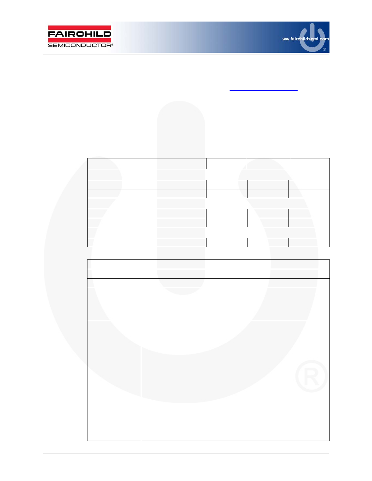
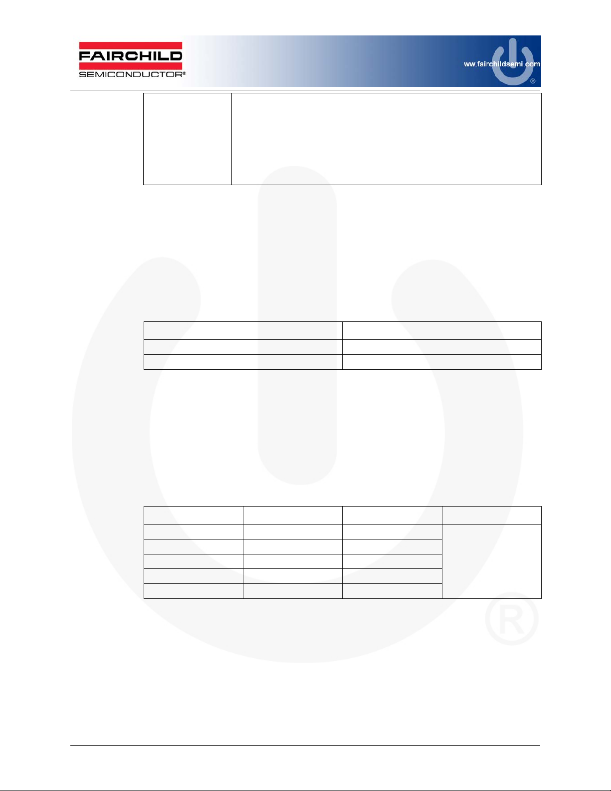
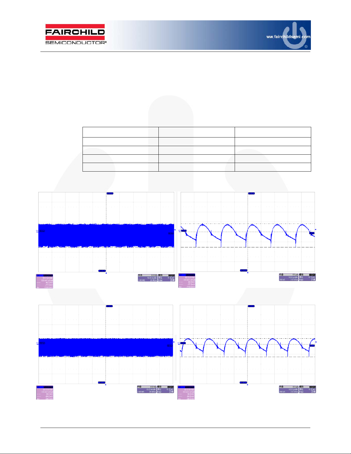
3.3. Measured Waveform
Figure 1. 90V / 60Hz at No Load, Ch1: VDD, Ch4: VDS
Figure 2. 264V / 50Hz at No Load, Ch1: VDD, Ch4: VDS
© 2011 Fairchild Semiconductor Corporation 6 FEBFAN6920MR_T02U120A • Rev. 1.0.0
Page 7
4. Turn-On Time
4.1. Test Condition
Set output at maximum loading. Measure the interval between AC plug-in and
stable output.
4.2. Test Result
Input Voltage Turn-On Time (s)
90V / 60Hz 1.563
264V / 50Hz 0.914
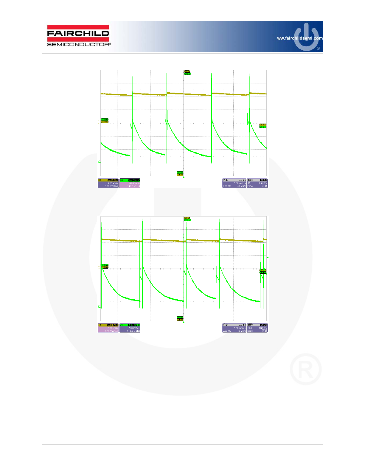
4.3. Measured Waveform
Figure 3. 90V / 60Hz at Maximum Load, Ch1:V
Ch4:VAC
O,
Figure 4. 264V / 50Hz at Maximum Load, Ch1:VO, Ch4:VAC
© 2011 Fairchild Semiconductor Corporation 7 FEBFAN6920MR_T02U120A • Rev. 1.0.0
Page 8
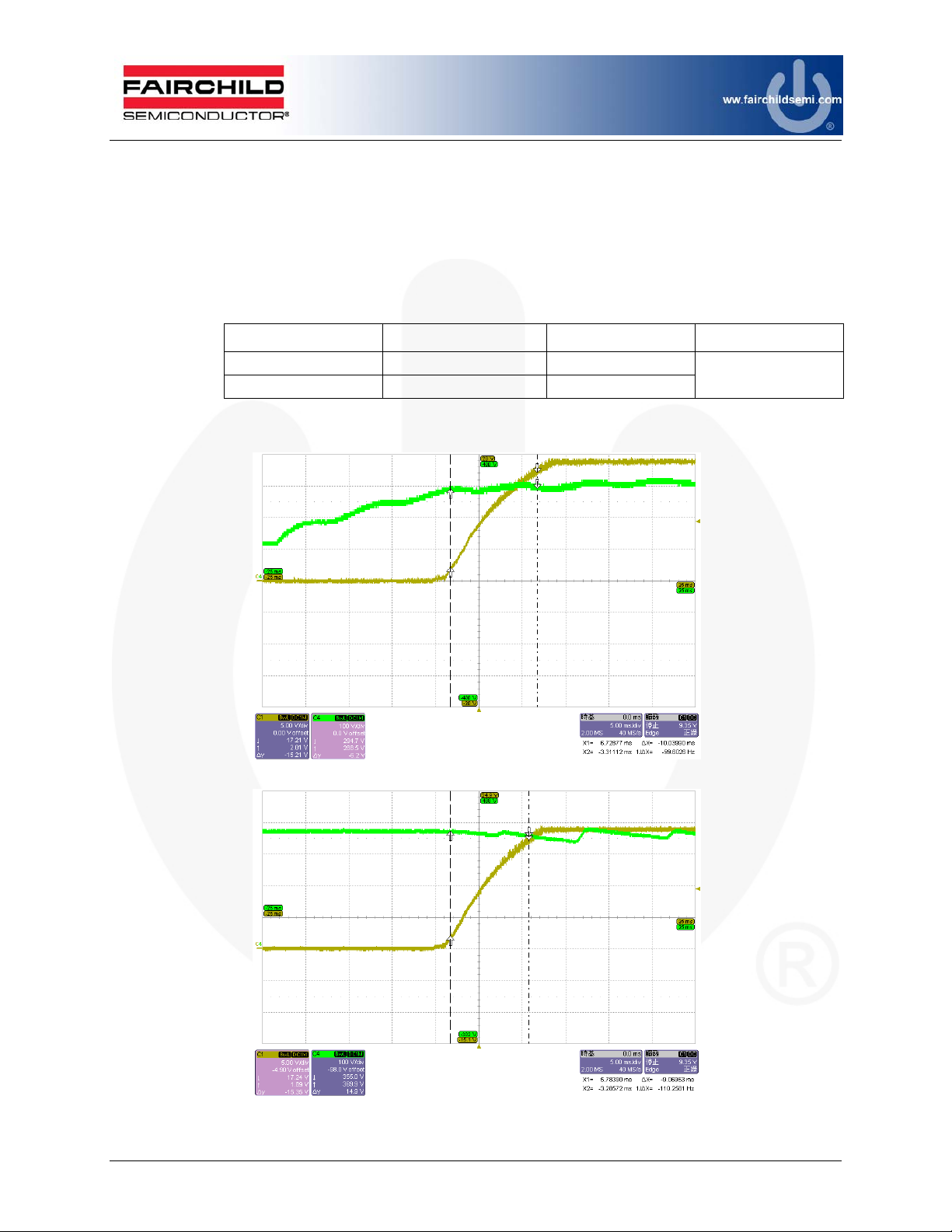
5. DC Output Rising Time
5.1. Test Condition
Set output at maximum loading. Measure the time interval between 10% and
90% output during startup.
5.2. Test Result
Input Voltage Maximum Load (ms) No Load (ms) Specification
90V / 60Hz 10.039 4.976
264V / 50Hz 9.070 4.583
5.3. Measured Waveform
<30ms
Figure 5. 90V / 60Hz at Maximum Load, Ch1: VO, Ch4: VDC
Figure 6. 264V / 50Hz at Maximum Load, Ch1: VO, Ch4: VDC
© 2011 Fairchild Semiconductor Corporation 8 FEBFAN6920MR_T02U120A • Rev. 1.0.0
Page 9
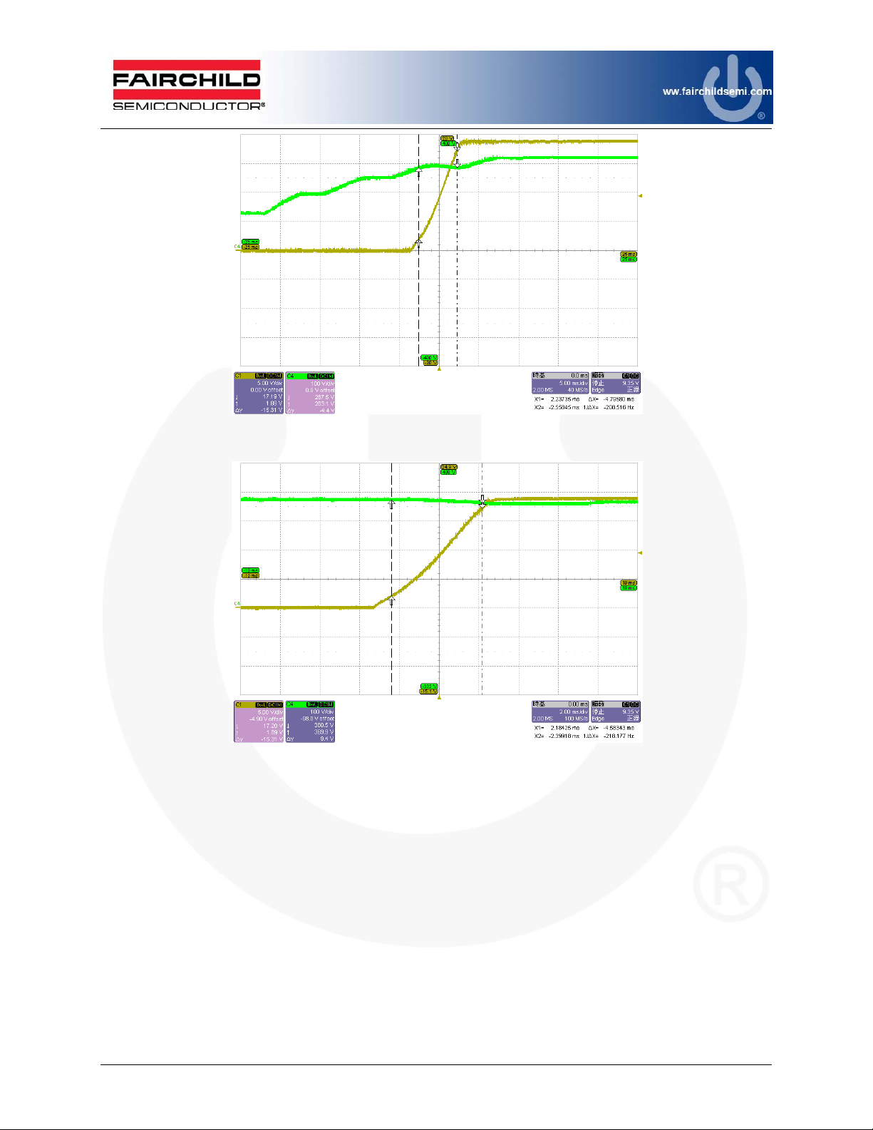
Figure 7. 90V / 60Hz at No Load, Ch1 VO, Ch4: VDC
Figure 8. 264V / 50Hz at No Load, Ch1: VO, Ch4: VDC
© 2011 Fairchild Semiconductor Corporation 9 FEBFAN6920MR_T02U120A • Rev. 1.0.0
Page 10
6. Line & Load Regulation
6.1. Test Condition
Measure line & load regulation according to the table below.
6.2. Test Result
7. Efficiency
7.1. Test Condition
Output at 25%, 50%, 75%, and 100% load.
7.2. Test Result
Input Voltage
90V / 60Hz 19.091 19.101 0.052
115V / 60Hz 19.090 19.100 0.052
132V / 60Hz 19.089 19.099 0.052
180V / 50Hz 19.084 19.098 0.073
230V / 50Hz 19.083 19.097 0.073
264V / 50Hz 19.083 19.097 0.073
Line Regulation (%) 0.042 0.021
Output Watt 30W 60W 90W 120W Avg. Specification
90V / 60Hz 87.61 90.84 90.78 90.02 89.81
115V / 60Hz 88.39 91.72 91.95 91.65 90.93
230V / 50Hz 91.92 91.54 92.64 93.15 92.31
264V / 50Hz 91.50 91.45 92.78 93.33 92.27
Output Voltage at
Maximum Load (V)
Output Voltage at
Minimum Load (V)
Load Regulation
(%)
>87%
© 2011 Fairchild Semiconductor Corporation 10 FEBFAN6920MR_T02U120A • Rev. 1.0.0
Page 11
8. Light-Load Specification
8.1. Test Condition
Output wattage at light load.
8.2. Test Result
Output Wattage Actual Output Wattage Input Wattage Specification
115V
0 0.166
0W
0.5W
1W
1.15W
1.5W
1.7W
AC
230VAC 0 0.184
115V
0.484 0.737
AC
230VAC 0.484 0.747
115V
0.998 1.348
AC
230VAC 0.994 1.303
115V
1.142 1.504
AC
230VAC 1.142 1.528
115V
1.486 1.902
AC
230VAC 1.486 1.934
115V
1.687 2.174
AC
230VAC 1.683 2.149
Input Watt <0.3W
Input Watt <1W
Input Watt <1.7W
Input Watt <2.16W
Input Watt <2.4W
Input Watt <2.4W
9. Light-Load Efficiency
9.1. Test Condition
Output efficiency at light load.
9.2. Test Result
Output Wattage Output Wattage Input Wattage Efficiency Specification
≤1W
≤1.7W
≤2.4W
≤14W
≤22W
115V
230VAC 0.994 1.303 76.29
115V
230VAC 1.683 2.149 78.32
115V
230VAC 2.398 2.985 80.34
115V
230VAC 14.000 15.900 88.05
115V
230VAC 21.990 24.570 89.50
0.998 1.348 74.03
AC
1.687 2.174 77.60
AC
2.377 2.984 79.66
AC
13.990 16.290 85.88
AC
21.970 25.150 87.36
AC
≥ 58%
≥ 68%
≥ 73%
≥ 83%
≥ 85%
© 2011 Fairchild Semiconductor Corporation 11 FEBFAN6920MR_T02U120A • Rev. 1.0.0
Page 12
10. Output Ripple & Noise
10.1. Test Condition
Ripple and noise are measured by using a 20MHz bandwidth-limited oscilloscope
with a 10F capacitor paralleled with a high-frequency 0.1F capacitor across
each output.
10.2. Test Result
Input Voltage Maximum Load (mV) Minimum Load (mV)
90V / 60Hz 91.6 27.4
115V / 60Hz 89.6 31.6
230V / 50Hz 78.6 31.6
264V / 50Hz 75.8 36.6
10.3. Measured Waveforms
Figure 9. 90V / 60Hz at Maximum Load, Ch3: VO
Figure 10. 264V / 50Hz at Maximum Load, Ch3: VO
© 2011 Fairchild Semiconductor Corporation 12 FEBFAN6920MR_T02U120A • Rev. 1.0.0
Page 13
11. Step Response
11.1. Test Condition
Dynamic loading (20%~80% of the full load, 5ms duty cycle, and 2.5A/µs rise /
fall time).
11.2. Test Result
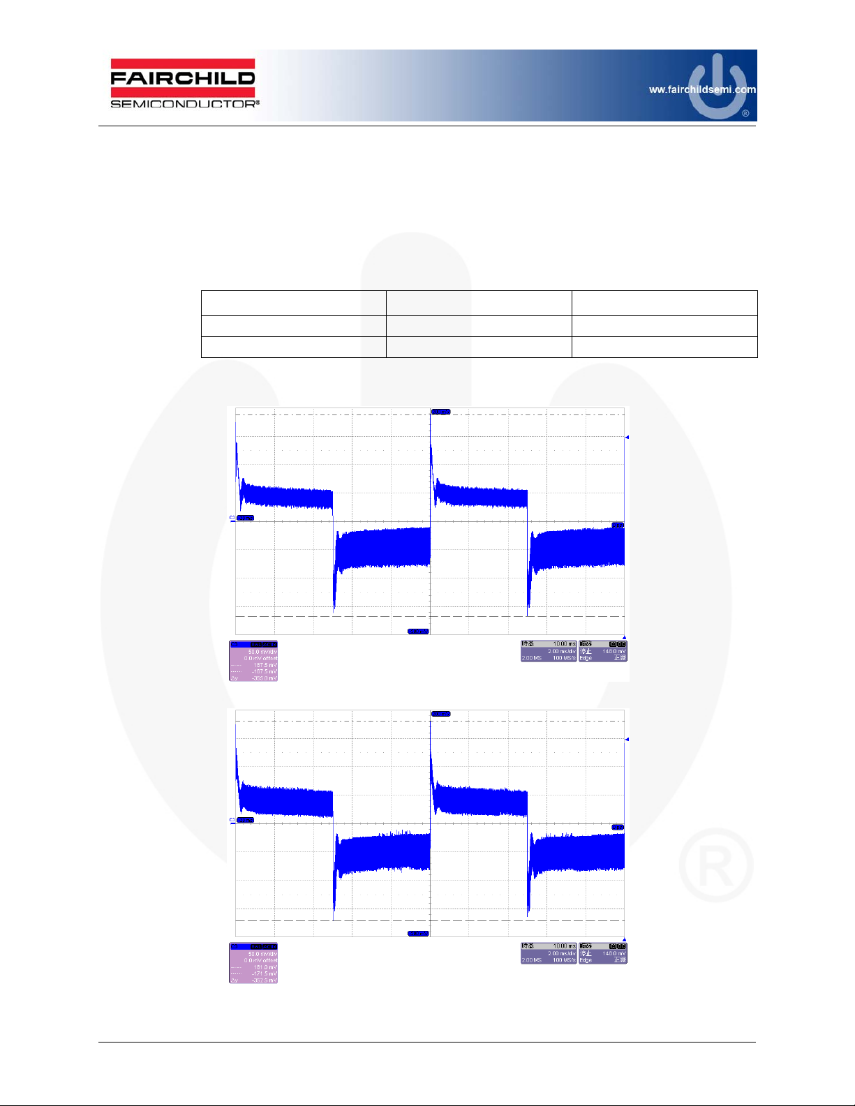
Input Voltage Overshoot (mV) Undershoot (mV)
115V / 60Hz 187.5 167.5
230V / 50Hz 181.5 171.5
11.3. Measured Waveform
Figure 11. 115V / 60Hz at Maximum Load, Ch3: VO
Figure 12. 230V/50Hz at Maximum Load, Ch3: VO
© 2011 Fairchild Semiconductor Corporation 13 FEBFAN6920MR_T02U120A • Rev. 1.0.0
Page 14
12. Over-Voltage Protection
/
12.1. Test Condition
Short the secondary side of opto-coupler at maximum load.
12.2. Test Result
Input Voltage Output Voltage (Maximum Value) (V)
115V/60Hz 23.4
230V/50Hz 23.4
12.3. Measured Waveform
Ch1: VO
Ch2:DET
Ch3:OPWM
Ch4:OPFC
Figure 13. 115V/60Hz at Maximum Load
Figure 14. 230V
50Hz at Maximum Load
Ch1: VO
Ch2:DET
Ch3:OPWM
Ch4:OPFC
© 2011 Fairchild Semiconductor Corporation 14 FEBFAN6920MR_T02U120A • Rev. 1.0.0
Page 15
13. Over-Power Protection
13.1. Test Condition
Increase output loading gradually.
13.2. Test Result
Input Voltage Output Power (W) Output Current (A) Specification
90V/60Hz 156.01 8.236
115V/60Hz 155.78 8.221
230V/50Hz 168.24 8.880
264V/50Hz 168.45 8.865
14. Hold-Up Time
14.1. Test Condition
Set output at maximum load. Measure the time interval between AC off and
output voltage falling to the lower limit of the rated value. The AC waveform
should be off at zero degree.
>120%
<150% Full Load
14.2. Test Result
Input Voltage Hold-Up Time (ms)
90V / 60Hz 21.31
115V / 60Hz 20.80
230V / 50Hz 51.95
264V / 50Hz 51.95
© 2011 Fairchild Semiconductor Corporation 15 FEBFAN6920MR_T02U120A • Rev. 1.0.0
Page 16
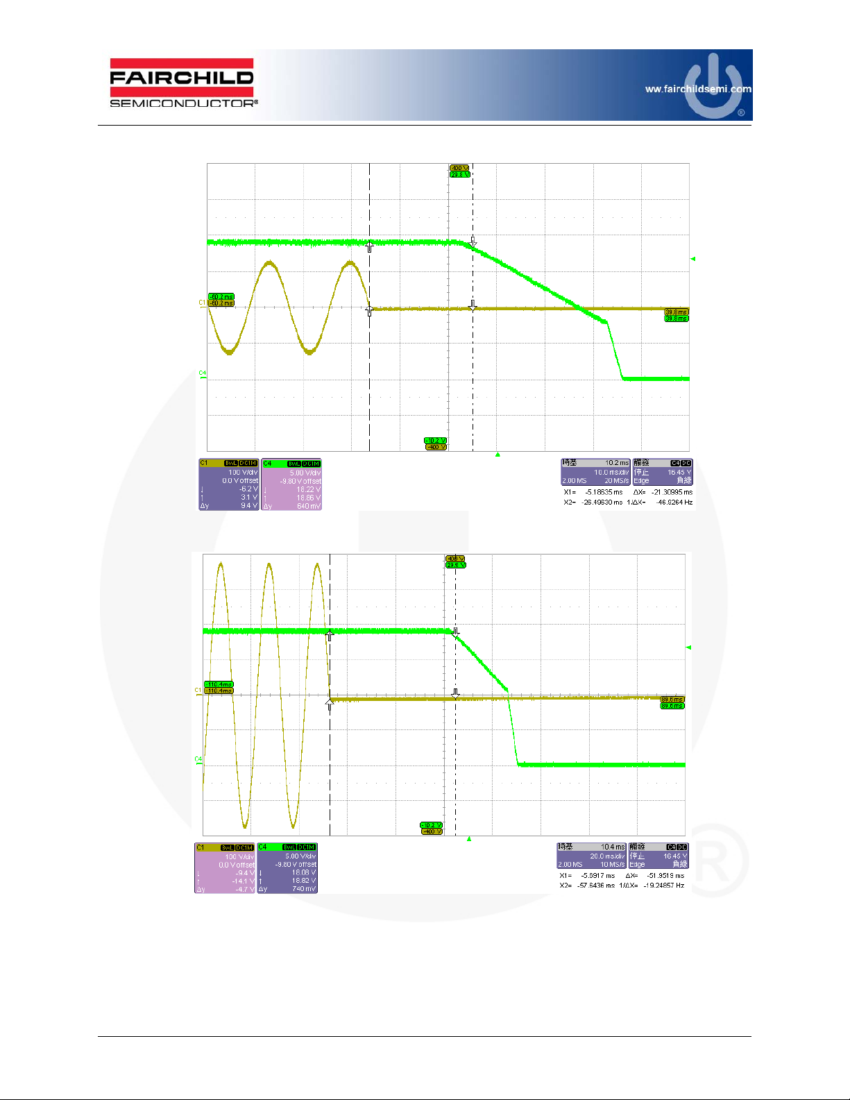
14.3. Measured Waveform
Figure 15. 90V/60Hz at Maximum Load
Ch4: VO
Ch1: V
AC
Figure 16. 264V / 50Hz at Maximum Load
Ch4: VO
Ch1: V
AC
© 2011 Fairchild Semiconductor Corporation 16 FEBFAN6920MR_T02U120A • Rev. 1.0.0
Page 17

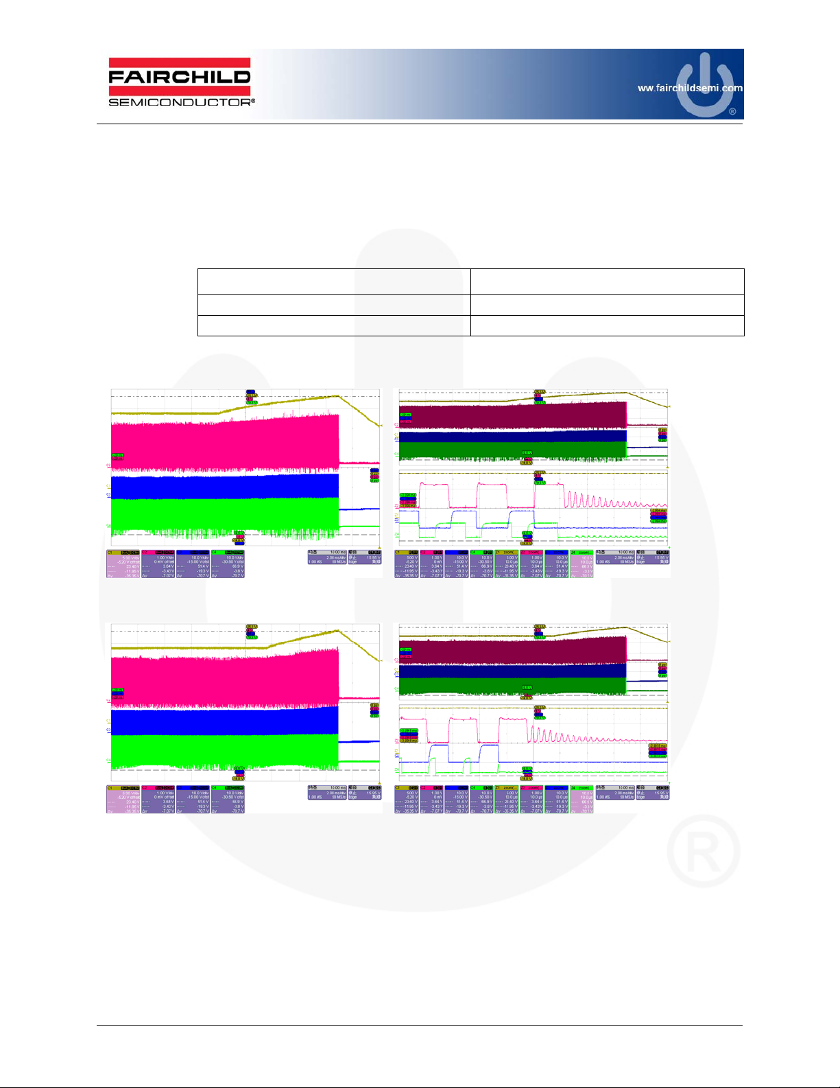
15. Short-Circuit Protection
/
/
15.1. Test Condition
Short the output of the power supply. The power supply should enter “Hiccup”
Mode protection with less than 2W input voltage.
15.2. Test Result
Input Voltage
90V/60Hz 1.231 1.25
264V/50Hz 1.344 1.45
Input Wattage at
Maximum Loading (W)
15.3. Measured Waveforms
Figure 17. 90V
Input Wattage at
Minimum Loading (W)
60Hz at Maximum Load
Specification
<2W
Ch2: VDD
Ch3: OPWM
Ch2: VDD
Ch3 OPWM
Figure 18. 264V
© 2011 Fairchild Semiconductor Corporation 17 FEBFAN6920MR_T02U120A • Rev. 1.0.0
50Hz at Maximum Load
Page 18

16. Brownout Test
16.1. Test Condition
Set output at maximum loading. Decrease input voltage with 5VAC step. Record
input wattage and output voltage. After the output is off, increase the AC voltage
gradually and record the recovery voltage.
16.2. Test Result
Input Voltage Input Wattage Output Voltage
90V / 60Hz 132.9 19.088
85V / 60Hz 133.5 19.088
80V / 60Hz 134.4 19.086
75V / 60Hz 135.4 19.084
70V / 60Hz 136.9 19.084
67V / 60Hz 0 0
Recovery voltage: 77 VAC
17. VDD Voltage Level
17.1. Test Result
Input Voltage Min. Load (V) Max. Load (V) Near OPP(V)
90V / 60Hz 10.35~11.65 16.40 17.35 11.65
264V / 50Hz 10.25~11.95 16.00 17.65 11.65
Output S.C.
(Max. Value) (V)
© 2011 Fairchild Semiconductor Corporation 18 FEBFAN6920MR_T02U120A • Rev. 1.0.0
Page 19

17.2. Measured Waveform
/
Figure 19. 90V/60Hz at Maximum Load
Ch2: VDD
Ch3: OPWM
Ch2: VDD
Ch4: CSPWM
Figure 20. 90V
© 2011 Fairchild Semiconductor Corporation 19 FEBFAN6920MR_T02U120A • Rev. 1.0.0
60Hz at Output Short Circuited
Page 20

Figure 21. 264V/50Hz at Maximum Load
/
Ch2: VDD
Ch3: OPWM
DD
Figure 22. 264V
Ch2: V
Ch3: OPWM
50Hz at Output Short Circuited
© 2011 Fairchild Semiconductor Corporation 20 FEBFAN6920MR_T02U120A • Rev. 1.0.0
Page 21

18. Voltage Stress on MOSFET & Rectifiers
18.1. Test Condition
Measure the voltage stress on MOSFET and secondary rectifiers under below
specified conditions.
18.2. Test Result
Input Voltage
90V / 60Hz, Max. Load 338
90V / 60Hz, Max. Load, Startup 365 57.4
90V / 60Hz, Max. Load, Output Short 379 62.0
264V / 50Hz, Max. Load 437 55.2
264V / 50Hz, Max. Load, Startup 442 66.2
264V / 50Hz, Max. Load, Output Short 456 70.2
264V / 50Hz, Max. Load, Turn Off 437 55.6
18.3. Measured Waveforms
Stress on
MOSFET (V)
Rating
600V
Stress on
Output Rectifier (V)
45.8
Ch1: V
Ch2: V
Rating
75V
DS_SR
DS_PWM
Figure 23. 264V/50Hz max load
© 2011 Fairchild Semiconductor Corporation 21 FEBFAN6920MR_T02U120A • Rev. 1.0.0
Page 22

f
Figure 24. 264V/50Hz Short circuit
Ch1: V
Ch2: V
Ch4: V
Ch1: V
Ch2: V
Ch4: VO
DS_SR
DS_PWM
O
DS_SR
DS_PWM
Figure 25. 264V/50Hz max load turn of
© 2011 Fairchild Semiconductor Corporation 22 FEBFAN6920MR_T02U120A • Rev. 1.0.0
Page 23

19. Current Har monic Test
19.1. Test Condition
Load: Pi=75W & maximum load.
19.2. Test Result
Input Voltage
90V / 60Hz
115V / 60Hz
240V / 50Hz
264V / 50Hz
Full Load
PF THD (%)
Pi=75W 0.997 4.84
Max. Load 0.999 2.97
Pi=75W 0.994 5.59
Max. Load 0.998 3.49
Pi=75W 0.947 13.69
Max. Load 0.979 7.54
Pi=75W 0.928 16.87
Max. Load 0.970 9.18
Specification
IEC1000-3-2
Class D
© 2011 Fairchild Semiconductor Corporation 23 FEBFAN6920MR_T02U120A • Rev. 1.0.0
Page 24

20. EMI Test
Figure 26. Conduction Line at 115VACFull Load Figure 27. Conduction Line at 230VAC Full Load
Figure 28. Conduction Neutral at 115VACFull Load Figure 29. Conduction Neutral at 230VAC Full Load
Figure 30. Conduction Line at 115VAC75% Load Figure 31. Conduction Line at 230VAC 75% Load
© 2011 Fairchild Semiconductor Corporation 24 FEBFAN6920MR_T02U120A • Rev. 1.0.0
Page 25

Figure 32. Conduction Neutral at 115VAC75% Load Figure 33. Conduction Neutral at 230VAC 75% Load
Figure 34. Conduction Line at 115VAC50% Load Figure 35. Conduction Line at 230VAC 50% Load
Figure 36. Conduction Neutral at 115VAC50% Load Figure 37. Conduction Neutral at 230VAC 50% Load
© 2011 Fairchild Semiconductor Corporation 25 FEBFAN6920MR_T02U120A • Rev. 1.0.0
Page 26

Figure 38. Conduction Line at 115VAC25% Load Figure 39. Conduction Line at 230VAC 25% Load
Figure 40. Conduction Neutral at 115VAC25% Load Figure 41. Conduction Neutral at 230VAC 25% Load
© 2011 Fairchild Semiconductor Corporation 26 FEBFAN6920MR_T02U120A • Rev. 1.0.0
Page 27

21. Surge Test
Mode Polarity Phase Voltage Condition
L-PE
N-PE
L-N
± 0∘
± 90∘ PASS
6KV
± 180∘ PASS
± 270∘ PASS
± 0∘
± 90∘ PASS
6KV
± 180∘ PASS
± 270∘ PASS
± 0∘
± 90∘ PASS
1KV
± 180∘ PASS
± 270∘ PASS
PASS
PASS
PASS
22. ESD Test
Air Discharge (16.5KV) Contact Discharge (8.8KV)
PASS PASS PASS PASS
© 2011 Fairchild Semiconductor Corporation 27 FEBFAN6920MR_T02U120A • Rev. 1.0.0
Page 28

23. System Reliability Test
No. Test Item Test Condition
= 264VAC
V
IN
= Room Temperature
T
A
Output – Press output short-circuit protect for 1 second and release for 1 second for
one test cycle (see Figure 42). Continue test cycle is 100 cycles.
1 cycle
Output
1.
Open/Short
1s 1s
Total 100 cycles
Figure 42. Output Open / Short Diagram
VIN = Power on 10s (264VAC); power off 30s
Power Supply
2.
ON/OFF
HighTemperature /
3.
High-Humidity
Operation
Low-
4.
Temperature
Operation
Low-
5.
Temperature
Starting Test
Output = Full Load
TA= 95°C
Test Time = 72 Hours
= 90VAC
V
IN
= 264VAC
V
IN
Output = Full Load
T
= 80°C
A
Humidity = 90%
Test Time = 24 Hours 24 Hours
= 90VAC
V
IN
= 264VAC
V
IN
T
= -5°C
A
Test Time = 24 Hours 24 Hours
= 90VAC
V
IN
= 264VAC
V
IN
Output = Full Load
Startup After 5°C / 2 Hours
Test
Result
Output open
PASS
Output short
PASS
PASS
PASS
PASS
PASS
PASS
PASS
© 2011 Fairchild Semiconductor Corporation 28 FEBFAN6920MR_T02U120A • Rev. 1.0.0
Page 29

24. Photographs
Figure 43. Top View
Figure 44. Lateral View
© 2011 Fairchild Semiconductor Corporation 29 FEBFAN6920MR_T02U120A • Rev. 1.0.0
Page 30

25. Schematic
Figure 45. Evaluation Board Schematic
© 2011 Fairchild Semiconductor Corporation 30 FEBFAN6920MR_T02U120A • Rev. 1.0.0
Page 31

26. Board Layout
Figure 46. Evaluation Board Layout (Mother Board), Top Overlay
Figure 47. Evaluation Board Layout (Mother Board), Bottom Overlay
Figure 48. Evaluation Board Layout (Mother Board), Bottom Layer
© 2011 Fairchild Semiconductor Corporation 31 FEBFAN6920MR_T02U120A • Rev. 1.0.0
Page 32

Figure 49. Evaluation Board Layout (Daughter Card), Top Overlay
Figure 50. Evaluation Board Layout (Daughter Card), Bottom Overlay
Figure 51. Evaluation Board Layout (Daughter Card), Bottom Layer
© 2011 Fairchild Semiconductor Corporation 32 FEBFAN6920MR_T02U120A • Rev. 1.0.0
Page 33

27. Bill of Materials, Main Board
Component Qty. Part No. Manufacturer Reference
JP6 JP1 JP10 JP7
JUMPER WIRE 0.8ψ(mm) 9
AC WIRE 1.5ψ(mm) 1 JP11
Non-Inductive Wire Wound Resistor 1W 0Ω27
±5%
SMD Resistor 0805 0Ω±5% 1 R27
SMD Resistor 0805 49.9Ω±5% 1 R17
SMD Resistor 0805 150Ω±5% 1 R18
SMD Resistor 0805 220Ω±5% 2 R7 R11
SMD Resistor 0805 330Ω±5% 1 R34
SMD Resistor 0805 560Ω±5% 1 R15
SMD Resistor 0805 1KΩ±5% 1 R36
SMD Resistor 0805 3.6KΩ±5% 1 R19
SMD Resistor 0805 8.25KΩ±1% 1 R23
SMD Resistor 0805 10KΩ±1% 2 R35 R38
SMD Resistor 0805 12.1KΩ±1% 1 R30
SMD Resistor 0805 16.2KΩ±1% 1 R32
SMD Resistor 0805 47.5KΩ±1% 1 R29
SMD Resistor 0805 66.5KΩ±1% 1 R37
SMD Resistor 0805 78.7KΩ±1% 1 R31
SMD Resistor 0805 165KΩ±1% 1 R16
SMD Resistor 0805 220KΩ±1% 1 R22
SMD Resistor 0805 249KΩ±1% 1 R8
SMD Resistor 1206 0Ω±5% 1 JP2
SMD Resistor 1206 49.9Ω±5% 2 R25 R26
SMD Resistor 1206 37.4KΩ±5% 2 R12 R13
SMD Resistor 1206 47.5KΩ±5% 1 R14
SMD Resistor 1206 100KΩ±5% 1 R33
SMD Resistor 1206 1.5MΩ±5% 2 R1 R2
SMD Resistor 1206 4.7MΩ±1% 4 R3 R4 R5 R6
SMD Resistor 2512 0.15 ±1% 2W 1 R20
NTC Thermistor 5ψ 100kΩ 1 TR1
SMD 0805 471P 50V ±10% 2 C11, C12
SMD 0805 102P 50V ±10% 2 C14, C17
SMD 0805 103P 50V ±10% 1 C23
SMD 0805 104P 50V ±10% 1 C9
SMD 0805 224P 50V ±10% 2 C13 C28
SMD 0805 105P 50V ±10% 1 C18
SMD 1206 102P 100V ±10% 1 C16
SMD 1206 103P 50V ±10% 1 C19
1 R21
JP9 JP8 JP3 JP4
JP5
© 2011 Fairchild Semiconductor Corporation 33 FEBFAN6920MR_T02U120A • Rev. 1.0.0
Page 34

Component Qty. Part No. Manufacturer Reference
SMD 1206 104P 50V ±10% 1 C8
Electrolytic Cap. 820µ 25V 105℃
Electrolytic Cap. 120µ 420V 105°C 1 PAG NCC C4
MPE Cap. 0.33µ 450V ±10% 1 C2
MPE Cap. 1µ 450V ±10% 1 C3
X1 Cap. 0.47µ 250V ±20% 1 C1
Y1 Cap. 102P/250V ±20% 1 C15
Bridge Rectifier 6A/600V 1 GBU6J Fairchild BD1
Ultra-Fast Diode 3A/600V DO-214AB 1 ES3J Fairchild D4
Ultra-Fast Diode 1A/600V DO-214AC 1 ES1J Fairchild D6
Ultra-Fast Diode 1A/1000V DO-41 1 UF1007 Fairchild D5
General-Purpose Rectifier 1A/1000V 2 S1M Fairchild D1 D2
Schottky Diode 1A/40V DO-41 1 1N5819 Fairchild D14
SMD Diode 1 LL4148 D3
SMD Zener Diode 1/2W 30V 1 MMSZ5256B Fairchild ZD3
PNP Transistor SOT-23 1 MMBT2907A Fairchild Q4
MOSFET 600V/16A TO-220 3 FCP16N60 Fairchild Q1 Q2 Q3
MOSFET 75V/235A TO-220 1 FDP032N08 Fairchild Q5
Filter Inductor 1 TRN0184 SEN HUEI L2
Common Mode Choke 1 FS1606H-1LB SHING GA L1
Choke 47nH 1 FP2-S047-R COOPER Bussmann L4
PFC Inductor RM10 400µH 1 TRN0321 SEN HUEI L3
PWM transformer POT-3319 1000µH 1 TRN0320 SEN HUEI TX1
Shunt Regulator ±2% 1 KA431SAMF2 Fairchild U4
Phototransistor Output Opto-coupler SMDIP-B 1 FOD817B Fairchild U3
FUSE GLASS 4A/250V QUICK 1 F1
Varistor 7ψ 470V 1 471KD07 MOV1
AC Inlet 2P 90° 1 CN1
Heat Sink (Primary) 1 MCH0646 HS1
Heat Sink (Secondary) 1 MCH0637 HS2
IC FAN6920MRMY 1 Fairchild U1
IC FAN6204MY 1 Fairchild U2
PCB PLM0178 V0 1 PCB
FAN7382 Card 1 CN2
3 KZH NCC C5 C6 C7
© 2011 Fairchild Semiconductor Corporation 34 FEBFAN6920MR_T02U120A • Rev. 1.0.0
Page 35

27.1. Bill of Materials, FAN7382 Card
Component Qty. Part No. Manufacturer Reference
SMD Resistor 0805 59Ω±1% 2 R32 R33
SMD Resistor 1206 0Ω±5% 3 R34 D10 D11
SMD 1206 104P 50V ±10% 1 C24
SMD 1206 105P 50V ±10% 1 C23
SMD Diode 2 LL4148 D9 D12
SMD Zener Diode 1/2W 20V 1 ZD2
Fast Recovery Rectifier 1A/200V, DO-41 2 1N4935 Fairchild D13 D14
Ultra Fast Diode 1A/1000V DO-41 1 UF1007 Fairchild D6
Electrolytic Cap. 47µ 50V 105°C 2 LHK JACKCON C25 C27
PIN HDR 1*8P 2.54mm 90° 1 CN3
IC FAN7382MX 1 Fairchild U4
PCB PLM0178-1 V0 1 PCB
© 2011 Fairchild Semiconductor Corporation 35 FEBFAN6920MR_T02U120A • Rev. 1.0.0
Page 36

28. Specification Approval
© 2011 Fairchild Semiconductor Corporation 36 FEBFAN6920MR_T02U120A • Rev. 1.0.0
Page 37

© 2011 Fairchild Semiconductor Corporation 37 FEBFAN6920MR_T02U120A • Rev. 1.0.0
Page 38

© 2011 Fairchild Semiconductor Corporation 38 FEBFAN6920MR_T02U120A • Rev. 1.0.0
Page 39

© 2011 Fairchild Semiconductor Corporation 39 FEBFAN6920MR_T02U120A • Rev. 1.0.0
Page 40

© 2011 Fairchild Semiconductor Corporation 40 FEBFAN6920MR_T02U120A • Rev. 1.0.0
Page 41

© 2011 Fairchild Semiconductor Corporation 41 FEBFAN6920MR_T02U120A • Rev. 1.0.0
Page 42

© 2011 Fairchild Semiconductor Corporation 42 FEBFAN6920MR_T02U120A • Rev. 1.0.0
Page 43

© 2011 Fairchild Semiconductor Corporation 43 FEBFAN6920MR_T02U120A • Rev. 1.0.0
Page 44

© 2011 Fairchild Semiconductor Corporation 44 FEBFAN6920MR_T02U120A • Rev. 1.0.0
Page 45

© 2011 Fairchild Semiconductor Corporation 45 FEBFAN6920MR_T02U120A • Rev. 1.0.0
Page 46

© 2011 Fairchild Semiconductor Corporation 46 FEBFAN6920MR_T02U120A • Rev. 1.0.0
Page 47

© 2011 Fairchild Semiconductor Corporation 47 FEBFAN6920MR_T02U120A • Rev. 1.0.0
Page 48

© 2011 Fairchild Semiconductor Corporation 48 FEBFAN6920MR_T02U120A • Rev. 1.0.0
Page 49

© 2011 Fairchild Semiconductor Corporation 49 FEBFAN6920MR_T02U120A • Rev. 1.0.0
Page 50

29. Revision History
Rev. Date Description
1.0.0 2/2012 Initial release
WARNING AND DISCLAIMER
Replace components on the Evaluation Board only with those parts shown on the parts list (or Bill of Materials) in the Users’ Guide. Contact an
authorized Fairchild representative with any questions.
This board is intended to be used by certified professionals, in a lab environment, following proper safety procedures. Use at your own risk. The
Evaluation board (or kit) is for demonstration purposes only and neither the Board nor this User’s Guide constitute a sales contract or create any kind
of warranty, whether express or implied, as to the applications or products involved. Fairchild warrantees that its products meet Fairchild’s published
specifications, but does not guarantee that its products work in any specific application. Fairchild reserves the right to make changes without notice to
any products described herein to improve reliability, function, or design. Either the applicable sales contract signed by Fairchild and Buyer or, if no
contract exists, Fairchild’s standard Terms and Conditions on the back of Fairchild invoices, govern the terms of sale of the products described herein.
DISCLAIMER
FAIRCHILD SEMICONDUCTOR RESERVES THE RIGHT TO MAKE CHANGES WITHOUT FURTHER NOTICE TO ANY PRODUCTS HEREIN TO
IMPROVE RELIABILITY, FUNCTION, OR DESIGN. FAIRCHILD DOES NOT ASSUME ANY LIABILITY ARISING OUT OF THE APPLICATION OR
USE OF ANY PRODUCT OR CIRCUIT DESCRIBED HEREIN; NEITHER DOES IT CONVEY ANY LICENSE UNDER ITS PATENT RIGHTS, NOR
THE RIGHTS OF OTHERS.
LIFE SUPPORT POLICY
FAIRCHILD’S PRODUCTS ARE NOT AUTHORIZED FOR USE AS CRITICAL COMPONENTS IN LIFE SUPPORT DEVICES OR SYSTEMS
WITHOUT THE EXPRESS WRITTEN APPROVAL OF THE PRESIDENT OF FAIRCHILD SEMICONDUCTOR CORPORATION.
As used herein:
1. Life support devices or systems are devices or systems which, (a)
are intended for surgical implant into the body, or (b) support or
sustain life, or (c) whose failure to perform when properly used in
accordance with instructions for use provided in the labeling, can be
reasonably expected to result in significant injury to the user.
ANTI-COUNTERFEITING POLICY
Fairchild Semiconductor Corporation's Anti-Counterfeiting Policy. Fairchild's Anti-Counterfeiting Policy is also stated on our external website,
www.fairchildsemi.com, under Sales Support.
Counterfeiting of semiconductor parts is a growing problem in the industry. All manufacturers of semiconductor products are experiencing
counterfeiting of their parts. Customers who inadvertently purchase counterfeit parts experience many problems such as loss of brand reputation,
substandard performance, failed applications, and increased cost of production and manufacturing delays. Fairchild is taking strong measures to
protect ourselves and our customers from the proliferation of counterfeit parts. Fairchild strongly encourages customers to purchase Fairchild parts
either directly from Fairchild or from Authorized Fairchild Distributors who are listed by country on our web page cited above. Products customers buy
either from Fairchild directly or from Authorized Fairchild Distributors are genuine parts, have full traceability, meet Fairchild's quality standards for
handling and storage and provide access to Fairchild's full range of up-to-date technical and product information. Fairchild and our Authorized
Distributors will stand behind all warranties and will appropriately address any warranty issues that may arise. Fairchild will not provide any warranty
coverage or other assistance for parts bought from Unauthorized Sources. Fairchild is committed to combat this global problem and encourage our
customers to do their part in stopping this practice by buying direct or from authorized distributors.
EXPORT COMPLIANCE STATEMENT
These commodities, technology, or software were exported from the United States in accordance with the Export Administration Regulations for the
ultimate destination listed on the commercial invoice. Diversion contrary to U.S. law is prohibited.
U.S. origin products and products made with U.S. origin technology are subject to U.S Re-export laws. In the event of re-export, the user will be
responsible to ensure the appropriate U.S. export regulations are followed.
2. A critical component is any component of a life support device or
system whose failure to perform can be reasonably expected to
cause the failure of the life support device or system, or to affect its
safety or effectiveness.
© 2011 Fairchild Semiconductor Corporation 50 FEBFAN6920MR_T02U120A • Rev. 1.0.0
Page 51

Mouser Electronics
Authorized Distributor
Click to View Pricing, Inventory, Delivery & Lifecycle Information:
Fairchild Semiconductor:
FEBFAN6920MR_T02U120A
 Loading...