

Page 1

User Guide for
FEBFAN6604MR_CH11U65A
Evaluation Board
Fairchild Computing Notebook Adapter
Featured Fairchild Product:
FAN6604MR
Direct questions or comments
about this evaluation board to:
“Worldwide Direct Support”
Fairchild Semiconductor.com
© 2015 Fairchild Semiconductor Corporation FEBFAN6604MR_CH11U65A • Rev. 1.1
Page 2

Table of Contents
1. Introduction ............................................................................................................................... 3
2. Evaluation Board Specifications ............................................................................................... 4
3. Photographs............................................................................................................................... 5
4. Printed Circuit Board ................................................................................................................ 6
5. Schematic .................................................................................................................................. 7
6. Bill of Materials ........................................................................................................................ 8
7. Transformer and Winding Specifications ............................................................................... 10
8. Test Conditions & Test Equipment......................................................................................... 12
9. Performance of Evaluation Board ........................................................................................... 12
9.1. Input Power at No Load Condition .............................................................................. 122
9.2. Startup Time................................................................................................................... 13
9.3. Hold-up Time ................................................................................................................. 13
9.4. Input Current .................................................................................................................. 14
9.5. DC Output Rising Time ................................................................................................. 14
9.6. Dynamic Response......................................................................................................... 15
9.7. Output Ripple & Noise .................................................................................................. 15
9.8. VDD Voltage Level ....................................................................................................... 16
9.9. Overload Protection (OLP) ............................................................................................ 16
9.10. Voltage Stress on MOSFET & Rectifiers ...................................................................... 17
9.11. Line & Load Regulation ................................................................................................ 17
9.12. Efficiency ....................................................................................................................... 18
9.13. Over-Current Protection (OCP) ..................................................................................... 19
9.14. Conducted Electromagnetic Interference (EMI) .......................................................... 220
9.15. Surge Test ...................................................................................................................... 21
9.16. ESD Test ........................................................................................................................ 21
10. Revision History ..................................................................................................................... 22
© 2015 Fairchild Semiconductor Corporation 2 FEBFAN6604MR_CH11U65A • Rev. 1.1
Page 3

This user guide supports the evaluation kit for the FAN6604MR. It should be used in
conjunction with the FAN6604MR datasheets as well as Fairchild’s application notes and
technical support team. Please visit Fairchild’s website at https://www.fairchildsemi.com/
1. Introduction
This document is an engineering report describing a 65 W power supply using
FAN6604MR PWM controller. This power supply is targeted towards power adapters
and open-frame for consumer products.
With the internal high-voltage startup circuitry, the power loss due to bleeding resistors is
also eliminated. To further reduce power consumption, FAN6604MR is manufactured by
using the BiCMOS process. This allows an operating current of 1.7 mA and low startup
current of 30 μA. Built-in synchronized slope compensation ensures the stability of Peak
Current Mode control.
© 2015 Fairchild Semiconductor Corporation 3 FEBFAN6604MR_CH11U65A • Rev. 1.1
Page 4
Specification
Min.
Max.
Unit
Input Voltage
90
264
VAC
Input Frequency
47
63
Hz
Description
Design Spec.
Test Results
Comments
Output Voltage
18.05 ~ 19.95 V
±0.08%
CV<± 5% Regulation
CC<±5% Regulation
Output Current
Protection
4.1 ~ 5.1 A
4.635 ~ 4.783 A
Input Power
< 100 mW
90 mW
264 VAC
Ripple
< 250 mVp-p
101 mVp-p (Max.)
Measured at PCB End
Startup Time
< 3 S
2.3 S
Full Load
Dynamic
> 18.5 V
18.83 V
Measure at PCB End
Voltage Stress
600 V
584 V
264 VAC
150 V
124 V
Efficiency
Avg. > 87%
87.9 % at 115 VAC
88.5 % at 230 VAC
Meets Energy Star v2.0
Conducted EMI
Under 6 dB
3 dB Margin
Meets
CISPER22B/EN55022B/IE
C950/UL1950 Class II
2. Evaluation Board Specifications
The data for Table 1 was measured with 90 VAC~264 VAC line input at an ambient temperature of 25°C.
Table 1. Summary of Features and Performance
© 2015 Fairchild Semiconductor Corporation 4 FEBFAN6604MR_CH11U65A • Rev. 1.1
Page 5
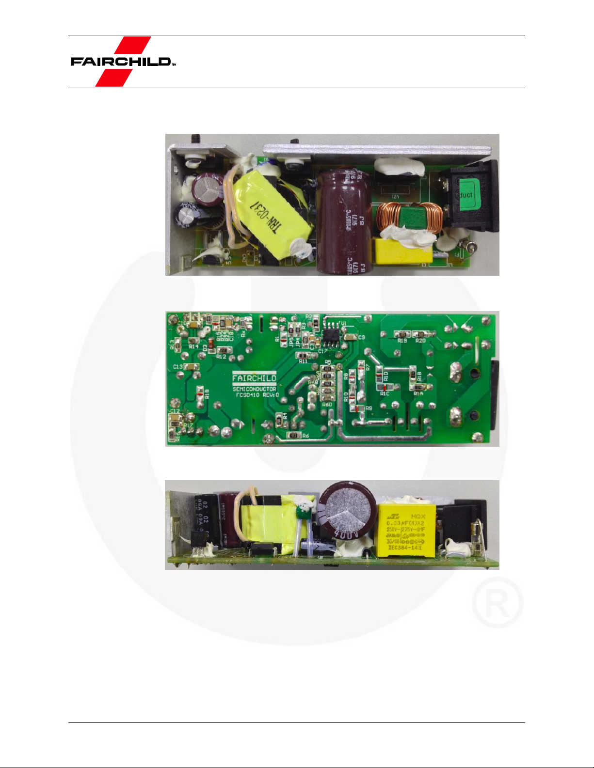
3. Photographs
Figure 1. Photograph (W x L: 40 x 103 mm2) Top View
Figure 2. Photograph (W x L: 40 x 103 mm2) Bottom View
Figure 3. Photograph (H:27 mm) Side View
© 2015 Fairchild Semiconductor Corporation 5 FEBFAN6604MR_CH11U65A • Rev. 1.1
Page 6
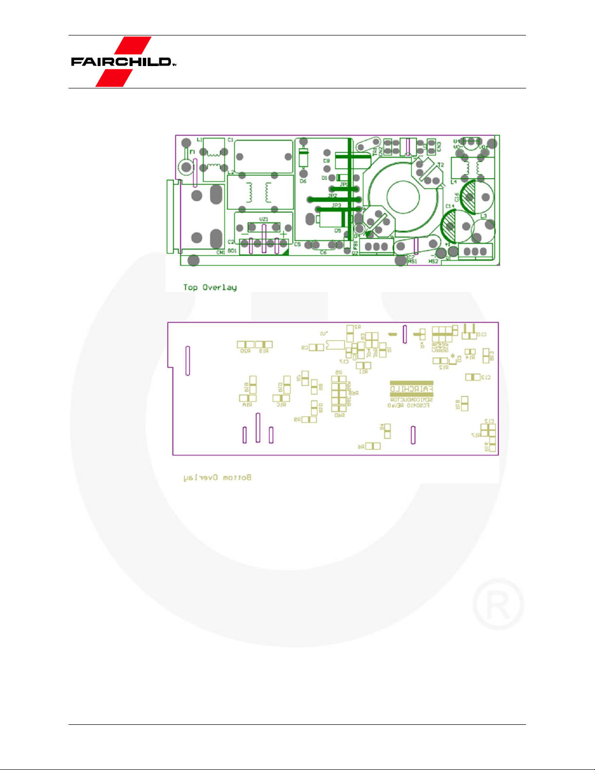
4. Printed Circuit Board
Figure 4. Top View
Figure 5. Bottom View
© 2015 Fairchild Semiconductor Corporation 6 FEBFAN6604MR_CH11U65A • Rev. 1.1
Page 7
1 2 3 4 5 6 7 8
A
B
C
D
87654321
D
C
B
A
Tit le
Doc.N o.
Prepared By
Reviewed By
Approved By
FAIRCHILD
SEMICONDUCTOR
SIZE
SHEE TRev.
Desc ripti on DAT E
0
INIT IAL
of
A3
1
2
CN1
CN/ 2 pin AC inlet
F1
F/4A/ 250 V
C2
XC/NC
+
C5
C/1 20u F/ 40 0V
R9
R/NC
C6
C/1 0nF /5 00 V
2
1
3
4
BD1
BD/2K BP06 M
2 1
D4
D/FR1 07
1
23
Q2
Q/ FQ P 8N 6 0C
R6A
R/1 .2R/ 12 06
GND1FB2NC3HV
4
RT
5
SEN SE
6
VDD
7
GAT E
8
U1
U/FAN66 04 MR
R4
R/2 0R/1 206
C3
C/1 nF/50 V/08 0 5
12
43
U3
U/FOD81 7A
R2
R/0 R/12 06
C12
C/1 nF/10 0V /12 06
R17
R/4 7R/1 206
R16
R/4 7R/1 206
1
3
2
Q1
Q/MBR 201 50C T
+
C14
C/1 000 uF /2 5V
R15
R/4 .7K/0 80 5
R14
R/3 0K/0 805
R13
R/2 00K/ 080 5
R12
R/1 .2K/1 20 6
C10
R/2 .2n F/50 V/12 06
+
C8
C/2 2uF /50 V
R10
R/NC
R6B
R/1 .2R/ 12 06
R6C
R/0 .5R/ 12 06
R6D
R/0 .5R/ 12 06
VZ1
VZ/NC
C1
XC /0.3 3u F /27 5V
1 2
34
L2
L/UU15 .5(9 mH)
4
976
5
T2
TX/RM-10
R3
R/5 .6K /1 206
C13
C/1 0nF /5 0V /12 06
VO+
VO-
R7
R/NC
R8
R/NC
C7
YC /22 nF /2 50 V
1 2
34
L1
L/SHORT
21
D5
TVS/P6 KE150 A
12
FB1
L/bead core
R11
R/0 R/12 06
+1
飛線
-1
飛線
+
C16
C/4 70u F/ 25 V
12
3 4
L4
L/SHORT
A K
R
U4
U/TL43 1
VO
R18
R/NC
1 2
L3
L/1.5u H
R1B
R/1 00K /12 0 6
VO
1
HS2
HS/1. 5X44 L
1
2
HS1
HS/3X 70
JP1
JP/7. 5mm
JP2
JP/15 mm
21
D1
D/IN493 5
C9
C/2 20p F/12 0 6
R5
R/1 00R /120 6
L
N
N1 N2
N3
N4
N5
N6
N7
N8
N9
N1 0
VDD
SEN SE
RTHVFBGAT E
N1 1
N1 3 N1 4
N1 5
N1 6
N1 7
+1
N1 9
N2 0
VO+
VO-
VB US
N2 1
N2 2 N23
GND VB US
R1D
R/NC
R1A
R/1 00K /12 0 6
R1C
R/NC
N5 A N4 A
R20
R/1 M/1 20 6
R19
R/1 M/120 6
TR1
TR/ 10 0K
C17
C/1 nF/50 V/08 0 5
N2 7
N2 8
JP3
JP/12 .5 mm
N6 GND
N2 4
JP4
R/0 R/08 05
JP5
R/0 R/08 05
21
D6
D/ IN 400 7
R6
R/4 7K/1 206
N2 9
Rx
R/6 .8K/0 80 5
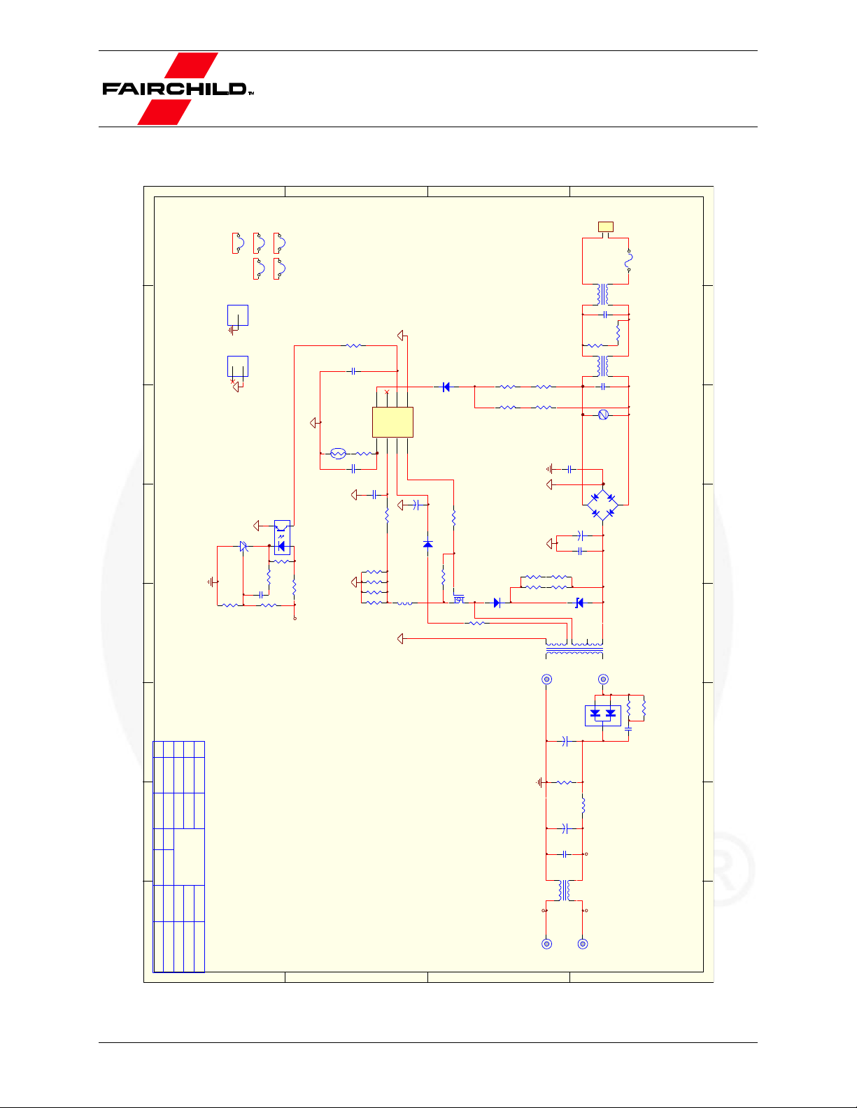
5. Schematic
Figure 6. Evaluation Board Schematic
© 2015 Fairchild Semiconductor Corporation 7 FEBFAN6604MR_CH11U65A • Rev. 1.1
Page 8

Part Specification
Package
Qty.
No.
JUMPER WIRE 0.8ψ(mm)
REEL
7
L1, L4, JP1, JP2, JP3
Chip Resistor 0805 0 Ω ±5%
REEL
1
JP4
Chip Resistor 0805 4K7 Ω ±1%
REEL
1
R15
Chip Resistor 0805 6K8 Ω ±5%
REEL
1
Rx
Chip Resistor 0805 30 KΩ ±5%
REEL
1
R14
Chip Resistor 0805 200 KΩ ±5%
REEL
1
R13
Chip Resistor 1206 0 Ω ±5%
REEL
2
R2, R11
Chip Resistor 1206 0 Ω 5 ±5%
REEL
2
R6C, R6D
Chip Resistor 1206 1 Ω 2 ±5%
REEL
2
R6A, R6B
Chip Resistor 1206 20 Ω ±5%
REEL
1
R4
Chip Resistor 1206 47 Ω ±5%
REEL
2
R16, R17
Chip Resistor 1206 100 Ω ±5%
REEL
1
R5
Chip Resistor 1206 1K2 Ω ±5%
REEL
1
R12
Chip Resistor 1206 5K6 Ω ±1%
REEL
1
R3
Chip Resistor 1206 47 KΩ ±5%
REEL
1
R6
Chip Resistor 1206 100 KΩ ±5%
REEL
2
R1A, R1B
Chip Resistor 1206 1 MΩ ±5%
REEL
2
R19, R20
NTC 5ψ 100000 Ω
REEL
1
TR1
Ceramic Capacitor 103P 500 V +80/-20%
REEL
1
C6
0805 MLCC X7R ±10% 102P 50 V
REEL
2
C3, C17
1206 MLCC X7R ±10% 102P 100 V
REEL
1
C12
1206 MLCC X7R ±10% 103P 50 V
REEL
1
C13
1206 MLCC X7R ±10% 221P 50 V
REEL
1
C9
1206 MLCC X7R ±10% 222P 50 V
REEL
1
C10
Electrolytic Capacitor 22 µ 50 V 105°C
JACKCON
1
C8
Electrolytic Capacitor 120 µ 400 V 105°C
NCC
1
C5
Electrolytic Capacitor 470 µ 25 V 105°C
NCC
1
C16
Electrolytic Capacitor 1000 µ 25 V 105°C
NCC
1
C14
X2 Capacitor 0.33 µ 275 V ±20%
REEL
1
C1
Y2 Capacitor 222P 250 V ±20%
REEL
1
C7
Inductor 1.7 µH
SUMIDA (74M-431)
1
L3
Common Choke 9 mH
SUMIDA (04291-T144)
1
L2
Bead Core C8B 3.5*3.2*1.0+T
MCH0041 (REEL)
1
FB1
Bead Core C8B 3.5*3.2*1.0
MCH0040
2
D4, C7
6. Bill of Materials
© 2015 Fairchild Semiconductor Corporation 8 FEBFAN6604MR_CH11U65A • Rev. 1.1
Continued on the following page…
Page 9

Part Specification
Package
Qty.
No.
Transformer RM-10 510 µH
SUMIDA (PS15-020)
1
T2
Diode 1 A/20 V
1N4935 (DO-41)
1
D1
Fast Diode 1 A/1000 V
FR107
1
D4
Diode 1 A/1000 V
1N4007
1
D6
Bridge 2 A/600 V
2KBP06M (Fairchild)
1
BD1
Schottky Diode 20 A/150 V
MBR20150CT (TO-220)
1
Q1
REGULATOR TL431ACZ-AP ±1%
TO-92
1
U4
MOSFET 8 A/600 V
FQP8N60C (TO-220)
1
Q2
IC FOD817A
DIP
2
U2, U3
FUSE GLASS 250V4A QUICK
REEL
1
F1
TVS P6KE150A
REEL
1
D5
INLET 2P 90°
1
CN1
PWM Controller IC SOIC
FAN6604MR 8-pin SOP
1
U1
Heat Sink 70 x 20 x 3.0 mm
MCH0534
1
HS1
Heat Sink 20 x 40 x 18 x 1.5 mm
MCH0555
1
HS2
CANADA Silicone ES2482W 333 ml
0
CN2, CN3, CN2A,
CN3A
PCB FCS0410 REV 0
1
© 2015 Fairchild Semiconductor Corporation 9 FEBFAN6604MR_CH11U65A • Rev. 1.1
Page 10

7. Transformer and Winding Specifications
Core: RM-10
Bobbin: RM-10
Figure 7. Transformer Specifications & Construction
© 2015 Fairchild Semiconductor Corporation 10 FEBFAN6604MR_CH11U65A • Rev. 1.1
Page 11

Winding
Terminal
Winding
Turns
Isolation Layer
Start Pin
End Pin
Turns
N4
5
6
0.5 mm*1
19
3
Copper Shielding (E2)
Open
4
Copper Foil
0.025 mm
1.2
3
N3
9
7
0.4 mm*1 7 1
N2
S
F
0.9 mm*1 8 3
Copper Shielding (E1)
Open
4
Copper Foil
0.025 mm
1.2
3
N1
4
5
0.5 mm*1
19
1
Pin
Specification
Remark
Inductance
4 - 6
510 µH ±10%
1 kHz, 1 V
Effective Leakage
4 - 6
20 µH Max.
Short Other Pin
Table 2. Winding Specifications
Table 3. Electrical Characteristics
© 2015 Fairchild Semiconductor Corporation 11 FEBFAN6604MR_CH11U65A • Rev. 1.1
Page 12

Evaluation Board #
FEBFAN6604MR_CH11U65A
Test Date
2014-10-28
Test Temperature
25℃
Test Equipments
AC Power Source: 6800 AC POWER SOURCE
Electronic Load: Chroma 63030 and 63102
Power Meter : WT210
Oscilloscope : LeCory 24Xs-A
Input Voltage
Input Wattage
Output Voltage
90 VAC / 60 Hz
44 mW
19.2 V
115 VAC / 60 Hz
47 mW
19.2 V
230 VAC / 50 Hz
79 mW
19.2 V
264 VAC / 50 Hz
90 mW
19.2 V
Figure 8. Input Wattage Curve
8. Test Conditions & Test Equipment
Table 4. Test Conditions & Test Equipment
9. Performance of Evaluation Board
9.1. Input Power at No Load Condition
Test Condition:
Measure the input power at three output voltage level at no load condition.
Table 5. Test Results
© 2015 Fairchild Semiconductor Corporation 12 FEBFAN6604MR_CH11U65A • Rev. 1.1
Page 13

Input Voltage
Startup Time
Specification
90 V
AC
/ 60 Hz
2.300 s
<3 sec
264 VAC / 50 Hz
0.758 s
Figure 9. C1[VIN], C4[Vo], 90 VAC / 60 Hz
Figure 10. C1[VIN], C4[Vo]. 264 VAC / 50 Hz
Input Voltage
Hold-up Time
Specification
90 VAC / 60 Hz
8.5 ms
264 VAC / 50 Hz
119.0 ms
Figure 11. C1[VIN], C4[VO], 90 VAC / 60 Hz
Figure 12. C1[VIN], C4[VO], 264 VAC /
50 Hz
9.2. Startup Time
Test Condition:
Measure the time from AC plug-in to nominal output voltage build-up at full load condition.
Table 6. Test Results
Waveform:
9.3. Hold-up Time
Test Condition:
Set output at maximum load. Measure the time interval between AC off and output voltage
falling to lower limit of rated value. The AC waveform should be off at zero degree.
Table 7. Test Results
Waveforms:
© 2015 Fairchild Semiconductor Corporation 13 FEBFAN6604MR_CH11U65A • Rev. 1.1
Page 14

Input Voltage
Input Current
Specification
90 VAC / 60 Hz
1.681 A
< 2 A
264 VAC / 50 Hz
0.680 A
Input Voltage
Minimum Load
Full Load
Specification
90 VAC/60 Hz
5.38 ms
9.40 ms
<20 ms
264 VAC/50 Hz
5.21 ms
8.86 ms
Figure 13. C4[VO], 90 VAC/60 Hz, Minimum Load
Figure 14. C4[VO], 90 VAC/60 Hz, Full Load
Figure 15. C4[VO], 264 VAC/50 Hz, Minimum Load
Figure 16. C4[VO] 264 VAC/50 Hz, Full Load
9.4. Input Current
Test Condition:
Measure the AC input current at maximum output loading, where the maximum input power
occurs.
Table 8. Test Results
9.5. DC Output Rising Time
Test Condition:
Measure the time interval between 10% to 90% of output voltage during startup.
Table 9. Test Results
Waveforms:
© 2015 Fairchild Semiconductor Corporation 14 FEBFAN6604MR_CH11U65A • Rev. 1.1
Page 15

Input Voltage
Overshoot
Undershoot
Specification
115 VAC/60 Hz
157 mV
163 mV
> V
230 VAC/50 Hz
141 mV
144 mV
Figure 17. C4[VO], 115 VAC / 60 Hz
Figure 18. C4[VO], 230 VAC / 50 Hz
Input Voltage
Full Load
Specification
90 VAC / 60 Hz
101 mV
P-P
<150 mV
P-P
115 VAC / 60 Hz
72 mV
P-P
230 VAC / 50 Hz
56 mV
P-P
264 VAC / 50 Hz
48 mV
P-P
Figure 19. C4[VO], 90 VAC / 60 Hz
Figure 20. C4[VO], 264 VAC / 50 Hz
9.6. Dynamic Response
Test Condition
Dynamic loading (0%~100%), 50% duty cycle (5 ms), 2.5 A/µsec rise/fall time. Measured at
PCB end.
Table 10. Test Results
Waveforms:
9.7. Output Ripple & Noise
Test Condition
Measure the output voltage ripple at full load condition at EVB end with 10 µF electrolytic
capacitor in parallel with 0.1 µF MLCC.
Table 11. Test Results
Waveforms:
© 2015 Fairchild Semiconductor Corporation 15 FEBFAN6604MR_CH11U65A • Rev. 1.1
Page 16

Input Voltage
Minimum Load
Maximum Load
Near OCP
Specification
90 VAC / 60 Hz
14.71 V
19.37 V
20.82 V
< 1 W
264 VAC / 50 Hz
14.40 V
18.53 V
19.63 V
Input Voltage
Minimum Load
Maximum Load
Specification
90 VAC / 60 Hz
54.8 ms
54.8 ms
264 VAC / 50 Hz
53 ms
55.1 ms
Figure 21. C1[FB], C2[GATE], C3[Vo], C4[VDD],
90 VAC/60 Hz
Figure 22. C1[FB], C2[GATE], C3[Vo], C4[VDD],
264 VAC/50 Hz
9.8. VDD Voltage Level
Test Condition
Measure VDD voltage at minimum, maximum loading and close over-current protection point.
Table 12. Test Results with Input Power
9.9. Overload Protection (OLP)
Test Condition:
Increase output loading gradually to trigger OLP and measure the debounce time.
Table 13. Test Results
Waveforms:
© 2015 Fairchild Semiconductor Corporation 16 FEBFAN6604MR_CH11U65A • Rev. 1.1
Page 17

90 VAC/ 60 Hz
264 VAC/ 50 Hz
Specification
Full Load
Full Load
Normal
MOSFET
326 V
584 V
VDS<650 V
VD<150 V
Rectifier
66.4 V
117 V
Short
Circuit
MOSFET
326 V
584 V
Rectifier
64.9 V
124 V
Waveforms:
Figure 23. C1[VDS], C2[VAK], 90 VAC/60 Hz,
Full Load Output Short
Figure 24. C1[VDS], C2[VAK], 264 VAC/50 Hz, Full
Load Output Short
Input Voltage
Output Voltage
at Maximum
Loading
Output Voltage
at Minimum
Loading
Load
Regulation
Specification
90 VAC / 60 Hz
19.144 V
19.16 V
0.08%
< ±5%
115 VAC / 60 Hz
19.146 V
19.16 V
0.07%
132 VAC / 60 Hz
19.146 V
19.16 V
0.07%
180 VAC / 50 Hz
19.146 V
19.16 V
0.07%
230 VAC / 50 Hz
19.148 V
19.162 V
0.07%
264 VAC / 50 Hz
19.148 V
19.162 V
0.07%
Line Regulation
0.02%
0.01%
9.10. Voltage Stress on MOSFET & Rectifiers
Test Condition
Measure the voltage and current stress on MOSFET and secondary rectifier under below the
conditions where the maximum voltage stress occurs.
Table 14. Test Results
9.11. Line & Load Regulation
Test Condition
Measure the line and load regulation according universal input and minimum to maximum
loading.
Table 15. Test Results with CC
© 2015 Fairchild Semiconductor Corporation 17 FEBFAN6604MR_CH11U65A • Rev. 1.1
Page 18

9.12. Efficiency
Input
Voltage
Output
Voltage
Output
Current
Input
Wattage
Efficiency
Average
Efficiency
90 VAC /
60 Hz
19.184 V
0.85 A
18.68 W
87.29%
86.55%
19.176 V
1.69 A
37.07 W
87.42%
19.172 V
2.546 A
56.44 W
86.48%
19.162 V
3.416 A
77.02 W
84.99%
115 VAC /
60 Hz
19.172 V
0.849 A
18.425 W
88.34%
87.90%
19.170 V
1.704 A
37.04 W
88.19%
19.160 V
2.545 A
55.55 W
87.78%
19.156 V
3.416 A
74.96 W
87.30%
230 VAC /
50 Hz
19.150 V
0.849 A
18.44 W
88.17%
88.51%
19.156 V
1.704 A
36.90 W
88.46%
19.150 V
2.544 A
55.01 W
88.56%
19.140 V
3.414 A
73.54 W
88.85%
264 VAC /
50 Hz
19.150 V
0.849 A
18.53 W
87.74%
88.22%
19.150 V
1.702 A
36.94 W
88.23%
19.148 V
2.544 A
55.03 W
88.52%
19.144 V
3.414 A
73.95 W
88.38%
Figure 25. 4 Points Efficiency Curve
115VAC 60Hz (87.90% avg)
230VAC 50Hz (88.51% avg)
Test Condition
Measure the efficiency at universal input voltage and maximum loading.
Table 16. Test Results
© 2015 Fairchild Semiconductor Corporation 18 FEBFAN6604MR_CH11U65A • Rev. 1.1
Page 19

Input Voltage
Over-Current Protection
Specification
90 VAC / 60 Hz
4.635 A
115 VAC / 60 Hz
4.783 A
230 VAC / 50 Hz
4.725 A
264 VAC / 50 Hz
4.657 A
Figure 26. Output Current Protection Curve
9.13. Over-Current Protection (OCP)
Test Condition
Increase output loading current gradually; and measure the output maximum current.
Table 17. Test Results
© 2015 Fairchild Semiconductor Corporation 19 FEBFAN6604MR_CH11U65A • Rev. 1.1
Page 20

Figure 27. Line: 115 VAC / 60 Hz
Figure 28. Neutral: 115 VAC / 60 Hz
Figure 29. Line: 230 VAC / 50 Hz
Figure 30. Neutral: 230 VAC / 50 Hz
15 0 kH z
30 M Hz
CLR WR
2 A V
CLR WR
dBµ V dBµ V
1 P K
RB W
9 k Hz
MT
1 0 ms
At t
1 0 dB
UNC ALUNC AL
1 MH z
10 M Hz
0
10
20
30
40
50
60
70
80
90
100
LI MI T CHEC K FAIL
LI NE E N550 22A FAIL
EN 55 02 2A
EN 55 02 2Q
Date: 1.JUN.2011 05:05:56
15 0 kH z
30 M Hz
CLR WR
2 A V
CLR WR
dBµ V dBµ V
1 P K
RB W
9 k Hz
MT
1 0 ms
At t
1 0 dB
UNC ALUNC AL
1 MH z
10 M Hz
0
10
20
30
40
50
60
70
80
90
100
EN 55 02 2A
EN 55 02 2Q
Date: 1.JUN.2011 05:13:44
15 0 kH z
30 M Hz
CLR WR
2 A V
CLR WR
dBµ V dBµ V
1 P K
RB W
9 k Hz
MT
1 0 ms
At t
1 0 dB
UNC ALUNC AL
1 MH z
10 M Hz
0
10
20
30
40
50
60
70
80
90
100
EN 55 02 2A
EN 55 02 2Q
Date: 1.JUN.2011 05:15:51
15 0 kH z
30 M Hz
CLR WR
2 A V
CLR WR
dBµ V dBµ V
1 P K
RB W
9 k Hz
MT
1 0 ms
At t
1 0 dB
UNC ALUNC AL
1 MH z
10 M Hz
0
10
20
30
40
50
60
70
80
90
100
EN 55 02 2A
EN 55 02 2Q
Date: 1.JUN.2011 05:21:12
9.14. Conducted Electromagnetic Interference (EMI)
Test Condition
Frequency Range: 150 kHz – 30 MHz, Probe: 2-Line-LISN ENV216
Signal Path: Receiver-2-Line-LISN ENV216, Detectors: Average
Output Load: 5.55
Test Results:
© 2015 Fairchild Semiconductor Corporation 20 FEBFAN6604MR_CH11U65A • Rev. 1.1
Page 21

L-PE
N-PE
L-N
Result
±4.4 kV
±4.4 kV
±1 kV
Air Discharge
Contact Discharge
Result
±16.5 kV
±8.8 kV
9.15. Surge Test
Test Condition
230 V
N-PE / L-PE: (Positive & Negative) 1 kV ~ 4 kV, Phase 0°, 90°, 180°, 270°.
L-N: (Positive & Negative) 500 V ~ 1 kV, Phase 0°, 90°, 180°, 270°.
Table 18. QC2.0 DP/DN Section Table
9.16. ESD Test
Test Condition:
230 V
Air discharge: (Positive & Negative) 8 kV ~ 16 kV, 20 times per level.
Contact discharge: (Positive & Negative) 4 kV ~ 8 kV, 20 times per level.
Table 19. Test Results
/ 50 Hz, maximum load.
AC
/ 50 Hz, maximum load.
AC
© 2015 Fairchild Semiconductor Corporation 21 FEBFAN6604MR_CH11U65A • Rev. 1.1
Page 22

Rev.
Date
Description
1.0
January 2015
Initial Release
1.1
June 2015
Table 1, 2, and 3 updated, BOM updated, Figure 7 replaced.
10. Revision History
WARNING AND DISCLAIMER
Replace components on the Evaluation Board only with those parts shown on the parts list (or Bill of Materials) in the Users’ Guide. Contact an
authorized Fairchild representative with any questions.
This board is intended to be used by certified professionals, in a lab environment, following proper safety procedures. Use at your own risk. The
Evaluation board (or kit) is for demonstration purposes only and neither the Board nor this User’s Guide constitute a sales contract or create any kind
of warranty, whether express or implied, as to the applications or products involved. Fairchild warrantees that its products meet Fairchild’s published
specifications, but does not guarantee that its products work in any specific application. Fairchild reserves the right to make changes without notice to
any products described herein to improve reliability, function, or design. Either the applicable sales contract signed by Fairchild and Buyer or, if no
contract exists, Fairchild’s standard Terms and Conditions on the back of Fairchild invoices, govern the terms of sale of the products described herein.
DISCLAIMER
FAIRCHILD SEMICONDUCTOR RESERVES THE RIGHT TO MAKE CHANGES WITHOUT FURTHER NOTICE TO ANY PRODUCTS HEREIN TO
IMPROVE RELIABILITY, FUNCTION, OR DESIGN. FAIRCHILD DOES NOT ASSUME ANY LIABILITY ARISING OUT OF THE APPLICATION OR
USE OF ANY PRODUCT OR CIRCUIT DESCRIBED HEREIN; NEITHER DOES IT CONVEY ANY LICENSE UNDER ITS PATENT RIGHTS, NOR
THE RIGHTS OF OTHERS.
LIFE SUPPORT POLICY
FAIRCHILD’S PRODUCTS ARE NOT AUTHORIZED FOR USE AS CRITICAL COMPONENTS IN LIFE SUPPORT DEVICES OR SYSTEMS
WITHOUT THE EXPRESS WRITTEN APPROVAL OF THE PRESIDENT OF FAIRCHILD SEMICONDUCTOR CORPORATION.
As used herein:
1. Life support devices or systems are devices or systems which, (a)
are intended for surgical implant into the body, or (b) support or
sustain life, or (c) whose failure to perform when properly used in
accordance with instructions for use provided in the labeling, can be
reasonably expected to result in significant injury to the user.
ANTI-COUNTERFEITING POLICY
Fairchild Semiconductor Corporation's Anti-Counterfeiting Policy. Fairchild's Anti-Counterfeiting Policy is also stated on our external website,
www.fairchildsemi.com, under Sales Support.
Counterfeiting of semiconductor parts is a growing problem in the industry. All manufacturers of semiconductor products are experiencing
counterfeiting of their parts. Customers who inadvertently purchase counterfeit parts experience many problems such as loss of brand reputation,
substandard performance, failed applications, and increased cost of production and manufacturing delays. Fairchild is taking strong measures to
protect ourselves and our customers from the proliferation of counterfeit parts. Fairchild strongly encourages customers to purchase Fairchild parts
either directly from Fairchild or from Authorized Fairchild Distributors who are listed by country on our web page cited above. Products customers buy
either from Fairchild directly or from Authorized Fairchild Distributors are genuine parts, have full traceability, meet Fairchild's quality standards for
handling and storage and provide access to Fairchild's full range of up-to-date technical and product information. Fairchild and our Authorized
Distributors will stand behind all warranties and will appropriately address any warranty issues that may arise. Fairchild will not provide any warranty
coverage or other assistance for parts bought from Unauthorized Sources. Fairchild is committed to combat this global problem and encourage our
customers to do their part in stopping this practice by buying direct or from authorized distributors.
EXPORT COMPLIANCE STATEMENT
These commodities, technology, or software were exported from the United States in accordance with the Export Administration Regulations for the
ultimate destination listed on the commercial invoice. Diversion contrary to U.S. law is prohibited.
U.S. origin products and products made with U.S. origin technology are subject to U.S Re-export laws. In the event of re-export, the user will be
responsible to ensure the appropriate U.S. export regulations are followed.
2. A critical component is any component of a life support device or
system whose failure to perform can be reasonably expected to
cause the failure of the life support device or system, or to affect its
safety or effectiveness.
© 2015 Fairchild Semiconductor Corporation 22 FEBFAN6604MR_CH11U65A • Rev. 1.1
 Loading...