April 2013
FDZ8040L — Integrated Load Switch
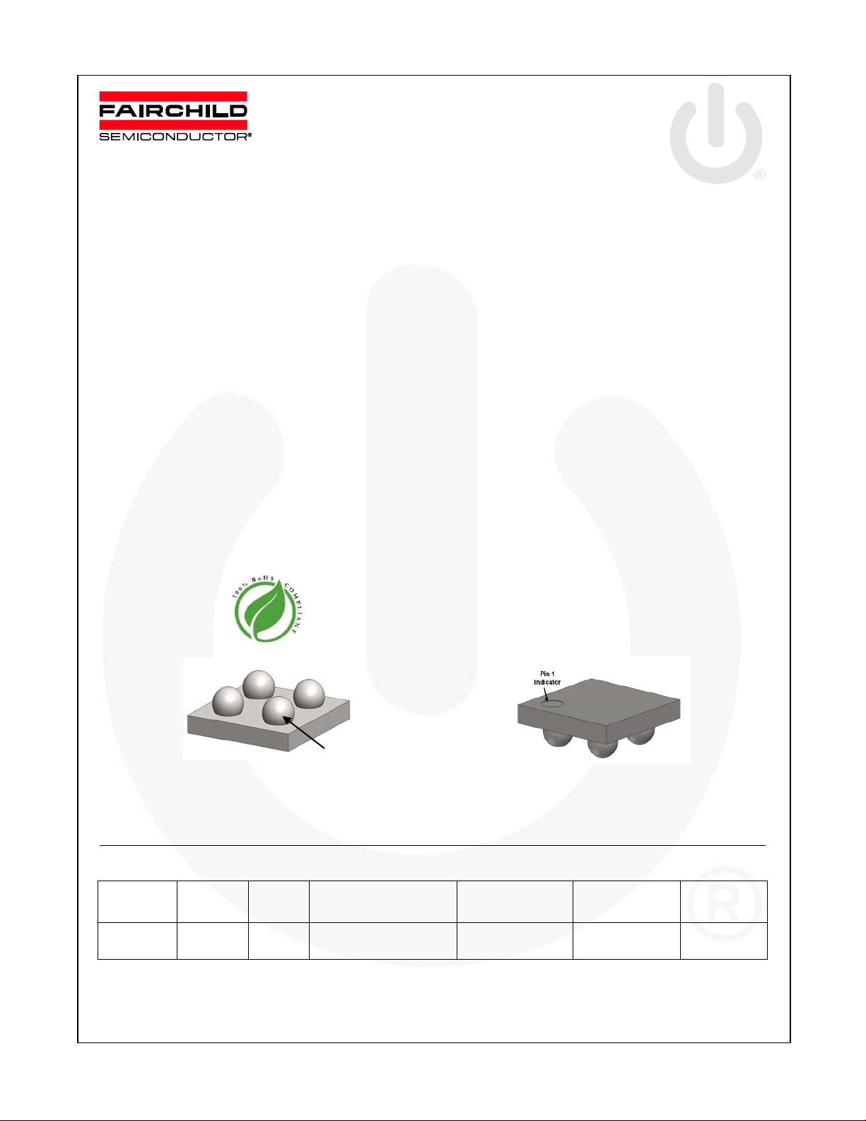
Figure 1. Bottom View
Figure 2. Top View
Part
Number
Device
Mark
Ball
Pitch
Operating
Temperature Range
Switch
Package
Packing
Method
FDZ8040L
ZM
0.4 mm
-40 to 85°C
80 m, P-Channel
MOSFET
0.8 x 0.8 x
0.5 mm3 WLCSP
Tape & Reel
Pin 1
VOUT
GND
ON
VIN
FDZ8040L
Integrated Load Switch
Features
Optimized for Low-Voltage Core ICs in
Portable Systems
Very Small Package Dimension: WLCSP
0.8 X 0.8 X 0.5 mm3
Current = 1.2 A, V
Current = 2 A, V
R
R
R
R
R
= 80 mΩ at VON = VIN = 4 V
DS(on)
= 85 mΩ at VON = VIN = 3.6 V
DS(on)
= 90 mΩ at VON = VIN = 3 V
DS(on)
= 360 mΩ at VON = VIN = 0.9 V
DS(on)
= 1000 mΩ at VON = VIN = 0.8 V
DS(on)
Max. = 4 V
IN
Max. = 4 V (Pulsed)
IN
RoHS Compliant
Description
This device is particularly suited for compact power
management in portable applications needing 0.8 V to
4 V input and 1.2 A output current capability. This load
switch integrated a level-shifting function that drives a Pchannel power MOSFET in a very small 0.8 X 0.8 X
0.5 mm3 WLCSP package.
Applications
Load Switch
Power Management in Portable Applications
Ordering Information
© 2011 Fairchild Semiconductor Corporation www.fairchildsemi.com
FDZ8040L • Rev. C1

FDZ8040L — Integrated Load Switch
OFF
ON
VIN
VOUT
ON
GND
VIN = 0.8 -4 V C
IN
C
OUT
FDZ8040L
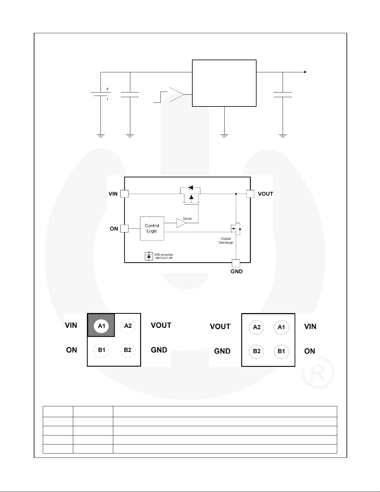
Figure 5. Top View (Bumps Down)
Figure 6. Bottom View (Bumps Up)
Pin #
Name
Description
A1
VIN
Supply Input: Input to the load switch
A2
VOUT
Switch Output: Output of the load switch
B1
ON
ON/OFF Control Input
B2
GND
Ground
Typical Application
Figure 3. Typical Application
Block Diagram
Pin Configuration
Pin Descriptions
© 2011 Fairchild Semiconductor Corporation www.fairchildsemi.com
FDZ8040L • Rev. C6 2
Figure 4. Internal Block Diagram

FDZ8040L — Integrated Load Switch
Symbol
Parameter
Min.
Max.
Unit
VIN
Voltage on VIN, VOUT, ON to GND
-0.3
4.2
V
I
OUT_C
I
OUT
-Load Current (Continuous)
(1a)
1.2
A
I
OUT_P
I
OUT
-Load Current (Pulsed)
2 A
PD
Power Dissipation at TA = 25°C
(1a)
0.9
W
TA
Operating Temperature Range
-40
85
°C
T
STG
Storage Temperature
-65
150
°C
R
ΘJA
Thermal Resistance, Junction to Ambient
(1a)
135
°C/W
ESD
Electrostatic Discharge Capability
Human Body Model, JESD22-A114
8
kV
Charged Device Model, JESD22-C101
2
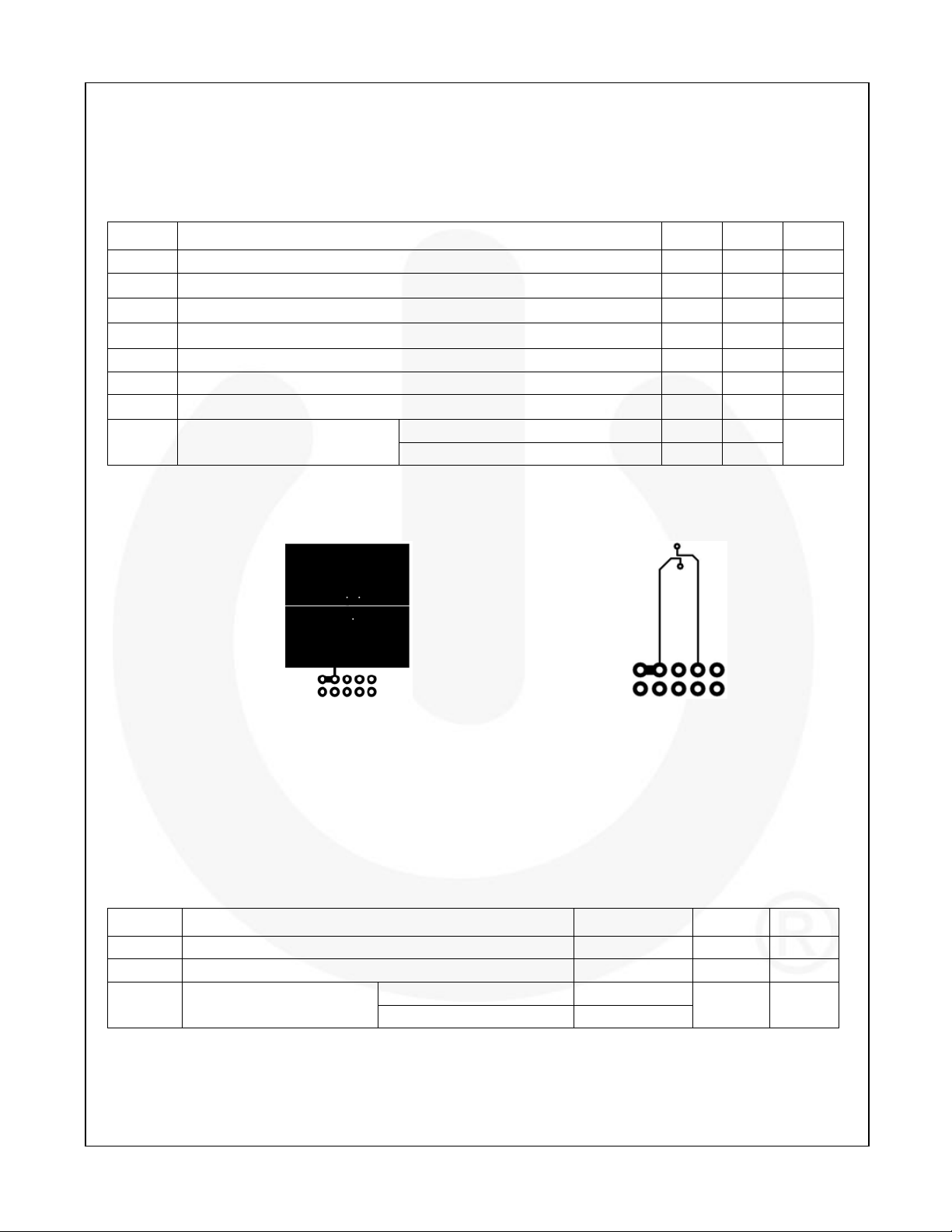
a. 135°C/W when mounted on a
1-inch square pad of 2-oz copper.
b. 360°C/W when mounted on a
minimum pad of 2-oz copper.
Symbol
Parameter
Min.
Max.
Unit
VIN
Voltage on VIN Pin
0.8
4.0
V
VON
Voltage on ON Pin
0.7
4.0
V
TA
Operating Temperature
Range
1 V to 4 V
-40
85
°C
0.8 V to 4 V
-10
Absolute Maximum Ratings
Stresses exceeding the absolute maximum ratings may damage the device. The device may not function or be
operable above the recommended operating conditions and stressing the parts to these levels is not recommended.
In addition, extended exposure to stresses above the recommended operating conditions may affect device reliability.
The absolute maximum ratings are stress ratings only.
Notes:
1. RΘJA is the sum of the junction-to-case and case-to-ambient thermal resistance where the case thermal
reference is defined as the solder mounting surface of the drain pins. RΘJC is guaranteed by design, while RΘJA
is determined by the board design.
2. Pulse test: pulse width < 300 µs; duty cycle < 2.0%.
Recommended Operating Conditions
The Recommended Operating Conditions table defines the conditions for actual device operation. Recommended
operating conditions are specified to ensure optimal performance to the datasheet specifications. Fairchild does not
recommend exceeding them or designing to Absolute Maximum Ratings.
© 2011 Fairchild Semiconductor Corporation www.fairchildsemi.com
FDZ8040L • Rev. C6 3

FDZ8040L — Integrated Load Switch
Symbol
Parameter
Test Conditions
Min.
Typ.
Max.
Unit
VIN
Operation Voltage
0.8 4.0
V
VIL
ON Input Logic Low Voltage
1.6 V ≤ VIN ≤ 4.0 V
0.35
V
0.8 V ≤ VIN ≤ 1.6 V
0.25
VIH
ON Input Logic High Voltage
1.6 V ≤ VIN ≤ 4.0 V
1.0
V
0.8 V ≤ VIN ≤ 1.6 V
0.7
IQ
Quiescent Current
I
OUT
= 0 mA, VIN = VON = 1.8 V
2.1
μA
I
Q(off)
Off Supply Current
I
OUT
= 0 mA, VIN = 1.8 V, VON = GND
1
μA
I
SD(off)
Off Switch Current
VON = GND, V
OUT
= 0 V, VIN = 1.8 V
100
nA
ION
ON Input Leakage
VON = VIN or GND
1
μA
RPD
Output Discharge Pull-Down
Resistance
200 Ω
R
DS(ON)
Static Drain-Source
On-Resistance
VON = VIN = 4 V, I
OUT
= 300 mA
50
80
mΩ
VON = VIN = 3.6 V, I
OUT
= 300 mA
51
85
VON = VIN = 3 V, I
OUT
= 300 mA
54
90
V
ON
= 0.7 V, V
IN
= 1.6 V, I
OUT
= 300 mA
73
110
V
ON
= 0.7 V, V
IN
= 1 V, I
OUT
= 300 mA
140
309
V
ON
= V
IN
= 0.9 V, I
OUT
= 10 mA
186
360
V
ON
= V
IN
= 0.8 V, I
OUT
= 10 mA
348
1000
V
ON
= V
IN
= 0.9 V, I
OUT
= 10 mA,
T
J
= 10 ~ 85°C
194
370
V
ON
= V
IN
= 0.8 V, I
OUT
= 10 mA,
T
J
= 10 ~ 85°C
268
750
V
IN
= 3.6 V, I
OUT
= 300 mA, T
J
= 85°C
59
102
Electrical Characteristics
TJ = 25°C and VIN=1.8 V, unless otherwise noted.
© 2011 Fairchild Semiconductor Corporation www.fairchildsemi.com
FDZ8040L • Rev. C6 4
 Loading...