Fairchild FDZ197PZ service manual

FDZ197PZ
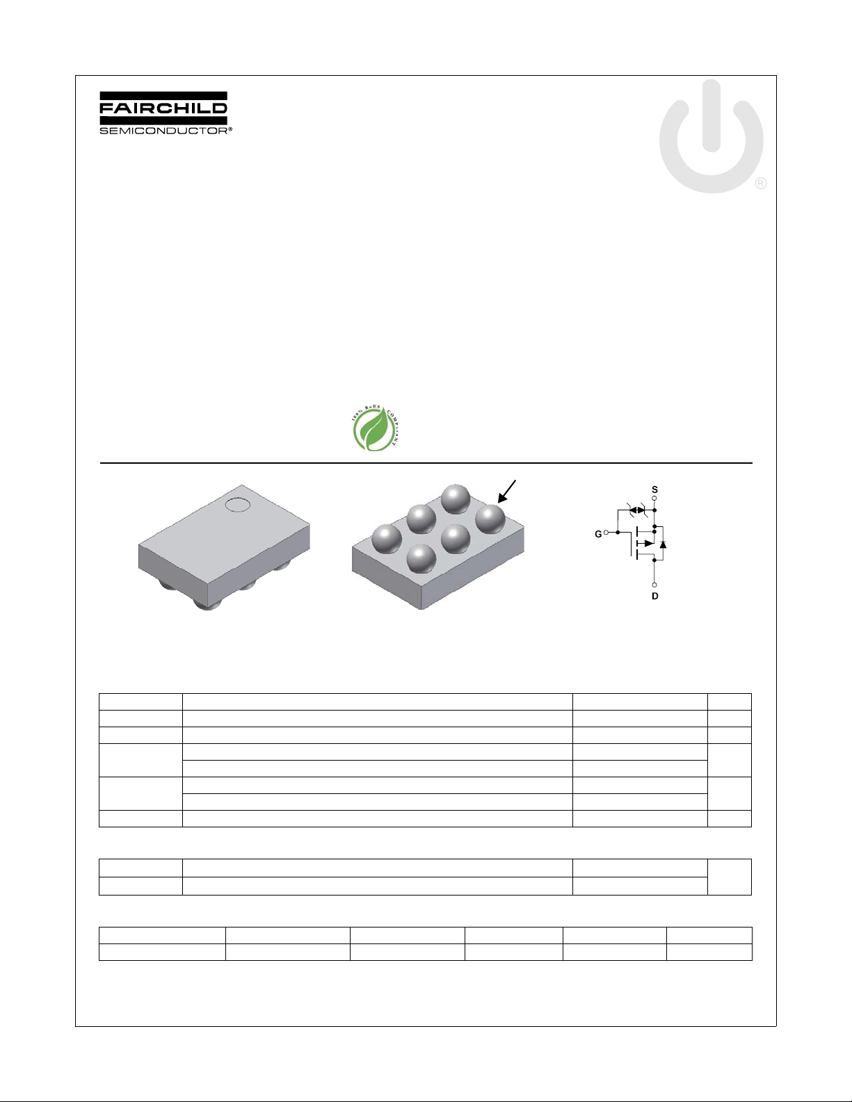
P-Channel 1.5 V Specified PowerTrench® Thin
-20 V, -3.8 A, 64 mΩ
Features
Max r
Max r
Max r
Max r
Occupies only 1.5 mm
area of 2 x 2 BGA
Ultra-thin package: less than 0.65 mm height when mounted
to PCB
HBM ESD protection level > 4400V (Note3)
RoHS Compliant
= 64 mΩ at VGS = -4.5 V, ID = -2.0 A
DS(on)
= 71 mΩ at VGS = -2.5 V, ID = -2.0 A
DS(on)
= 79 mΩ at VGS = -1.8 V, ID = -1.0 A
DS(on)
= 95 mΩ at VGS = -1.5 V, ID = -1.0 A
DS(on)
2
of PCB area.Less than 50% of the
General Description
Designed on Fairchild's advanced 1.5 V PowerTrench® process
with state of the art "fine pitch" WLCSP packaging process, the
FDZ197PZ minimizes both PCB space and r
advanced WLCSP MOSFET embodies a breakthrough in
packaging technology which enables the device to combine
excellent thermal transfer characteristics, ultra-low profile
packaging, low gate charge, and low r
Applications
Battery management
Load switch
Battery protection
WL-CSP MOSFET
.
DS(on)
June 2009
. This
DS(on)
FDZ197PZ P-Channel 1.5 V Specified PowerTrench
PIN1
S
S
D
D
TOP
WL-CSP 1x1.5 Thin
MOSFET Maximum Ratings T
Symbol Parameter Ratings Units
V
DS
V
GS
I
D
P
D
, T
T
J
STG
Drain to Source Voltage -20 V
Gate to Source Voltage ±8 V
-Continuous TA = 25°C (Note 1a) -3.8
-Pulsed -15
Power Dissipation TA = 25°C (Note 1a) 1.9
Power Dissipation T
Operating and Storage Junction Temperature Range -55 to +150 °C
= 25 °C unless otherwise noted
A
BOTTOM
A
G
S
= 25°C (Note 1b) 0.9
Thermal Characteristics
R
θJA
R
θJA
Thermal Resistance, Junction to Ambient (Note 1a) 65
Thermal Resistance, Junction to Ambient (Note 1b) 133
Package Marking and Ordering Information
A
W
°C/W
®
Thin
WL-CSP MOSFET
Device Marking Device Package Reel Size Tape Width Quantity
7 FDZ197PZ WL-CSP 1x1.5 Thin 7 ” 8 mm 5000 units
©2009 Fairchild Semiconductor Corporation
FDZ197PZ Rev.C1
1
www.fairchildsemi.com

Electrical Characteristics T
= 25 °C unless otherwise noted
J
Symbol Parameter Test Conditions Min Typ Max Units
Off Characteristics
BV
∆BV
∆T
I
DSS
I
GSS
DSS
DSS
J
Drain to Source Breakdown Voltage ID = -250 µA, VGS = 0 V -20 V
Breakdown Voltage Temperature
Coefficient
Zero Gate Voltage Drain Current VDS = -16 V, V
Gate to Source Leakage Current VGS = ±8 V, V
I
= -250 µA, referenced to 25 °C -10 mV/°C
D
= 0 V -1 µA
GS
= 0 V ±10 µA
DS
On Characteristics
V
GS(th)
∆V
∆T
r
DS(on)
g
FS
GS(th)
J
Gate to Source Threshold Voltage VGS = VDS, ID = -250 µA -0.4 -0.5 -1.0 V
Gate to Source Threshold Voltage
Temperature Coefficient
Static Drain to Source On Resistance
I
= -250 µA, referenced to 25 °C 2.7 mV/°C
D
V
= -4.5 V, ID = -2.0 A 46 64
GS
= -2.5 V, ID = -2.0 A 53 71
V
GS
= -1.8 V, ID = -1.0 A 59 79
V
GS
= -1.5 V, ID = -1.0 A 68 95
V
GS
= -4.5 V, ID = -2.0 A,
V
GS
T
=125 °C
J
54 84
Forward Transconductance VDD = -5 V, ID = -3.8 A 21 S
Dynamic Characteristics
C
iss
C
oss
C
rss
Input Capacitance
Output Capacitance 190 255 pF
Reverse Transfer Capacitance 160 225 pF
= -10 V, VGS = 0 V,
V
DS
f = 1 MHz
1180 1570 pF
mΩ
FDZ197PZ P-Channel 1.5 V Specified PowerTrench
®
Thin
Switching Characteristics
t
d(on)
t
r
t
d(off)
t
f
Q
Q
Q
g
gs
gd
Turn-On Delay Time
Rise Time 5.9 12 ns
Turn-Off Delay Time 311 498 ns
Fall Time 280 448 ns
Total Gate Charge V
Gate to Source Charge 1.5 nC
Gate to Drain “Miller” Charge 4.7 nC
= -10 V, ID = -3.8 A,
V
DD
V
= -4.5 V, R
GS
= 0V to -4.5V
GS
GEN
Drain-Source Diode Characteristics
V
SD
t
rr
Q
rr
Notes:
is determined with the device mounted on a 1 in2 pad 2 oz copper pad on a 1.5 x 1.5 in. board of FR-4 material. R
1. R
θJA
the user's board design.
Source to Drain Diode Forward Voltage V
Reverse Recovery Time
Reverse Recovery Charge 344 550 nC
a. 65 °C/W when mounted on
a 1 in2 pad of 2 oz copper.
= 0 V, IS = -1.1 A (Note 2) -0.6 -1.2 V
GS
= -3.8 A, di/dt = 100 A/µs
I
F
= 6 Ω
VDD
I
= -3.8 A
D
= -10 V,
5.8 12 ns
18 25 nC
194 310 ns
is guaranteed by desig n while R
θJC
b. 133 °C/W when mounted on a
minimum pad of 2 oz copper.
is determined by
θCA
WL-CSP MOSFET
2. Pulse Test: Pulse Width < 300µs, Duty cycle < 2.0%.
3. The diode connected between the gate and source serves only as protection ESD. No gate overvoltage rating is implied.
©2009 Fairchild Semiconductor Corporation
FDZ197PZ Rev.C1
2
www.fairchildsemi.com

Typical Characteristics T
= 25 °C unless otherwise noted
J
FDZ197PZ P-Channel 1.5 V Specified PowerTrench
15
12
9
6
DRAIN CURRENT (A)
,
D
3
-I
0
0123
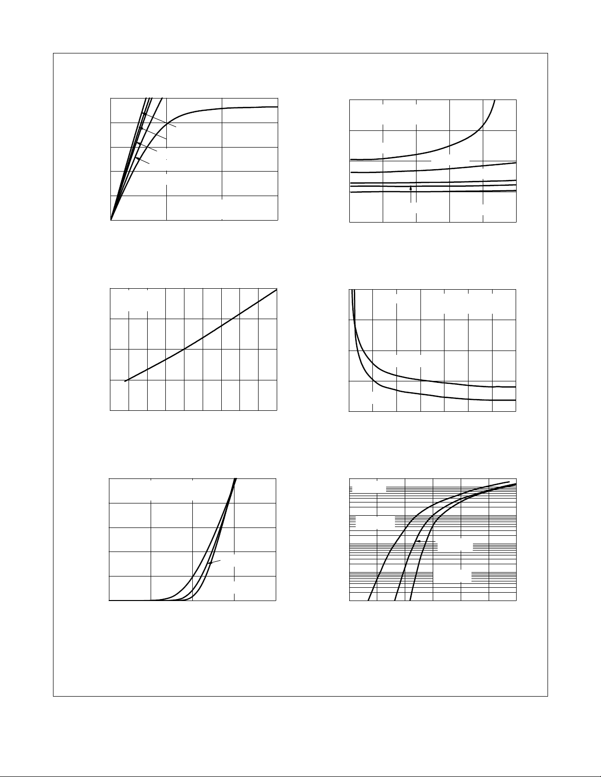
Figure 1.
1.4
ID = -2 A
V
= -4.5 V
GS
VGS = -1.5 V
-V
DS
On-Region Characteristics Figure 2.
VGS = -4.5 V
VGS = -3 V
VGS = -2.5 V
VGS = -1.8 V
PULSE DURATION = 80 µs
DUTY CYCLE = 0.5% MAX
,
DRAIN TO SOURCE VOLTAGE (V)
1.2
1.0
NORMALIZED
0.8
2.5
PULSE DURATION = 80 µs
DUTY CYCLE = 0.5% MAX
2.0
VGS = -1.5 V
1.5
NORMALIZED
VGS = -1.8 V
VGS = -2.5 V
1.0
DRAIN TO SOURCE ON-RESISTA NC E
0.5
03691215
VGS = -3 V
-I
,
DRAIN CURRENT (A)
D
VGS = -4.5 V
Norma l i z e d O n - Resistance
vs Drain Current and Gate Voltage
150
)
Ω
m
(
120
90
DRAIN TO
,
DS(on)
r
60
ID = -2 A
TJ = 125 oC
PULSE DURATION = 80 µs
DUTY CYCLE = 0.5% MAX
®
Thin
WL-CSP MOSFET
DRAIN TO SOURCE ON-RESISTANCE
0.6
-75 -50 -25 0 25 50 75 100 125 150
T
,
JUNCTION TEMPERATUR E
J
o
(
C
)
Figu r e 3. Nor m a lized O n - Resist a n ce
vs Junction Temperature
15
PULSE DURATION = 80 µs
DUTY CYCLE = 0.5% MAX
12
V
= -5 V
DS
9
6
, DRAIN CURRENT (A)
D
3
-I
0
0.0 0.5 1.0 1.5 2.0
TJ = 150 oC
-VGS, GATE TO SOURCE VO LTAGE (V)
TJ = 25 oC
TJ = -55 oC
Figure 5. Transfer Characteristics
TJ = 25 oC
SOURCE ON-RESISTANCE
30
1.0 1.5 2.0 2.5 3.0 3.5 4.0 4.5
-V
,
GATE TO SOURCE VOLTAGE (V)
GS
Figure 4.
On-Resistanc e v s Gate to
Source Voltage
20
V
= 0 V
GS
1
TJ = 150 oC
TJ = 25 oC
TJ = -55 oC
0.0 0.2 0.4 0.6 0.8 1.0 1.2
-VSD, BODY DIODE FORWARD VOLTAGE (V)
Figure 6.
Source to Dr ain Diode
0.01
, REVERSE DRAIN CURRENT (A)
S
-I
0.001
10
0.1
Forward Voltage vs Source Current
©2009 Fairchild Semiconductor Corporation
FDZ197PZ Rev.C1
3
www.fairchildsemi.com
 Loading...