Fairchild FDZ1905PZ service manual

July 2008
FDZ1905PZ Common Drain P-Channel 1.5V PowerTrench
FDZ1905PZ
Common Drain P-Channel 1.5V PowerTrench® WL-CSP MOSFET
–20V, –3A, 123mΩ
Features
Max r
Max r
Max r
Max r
Occupies only 1.5 mm2 of PCB area, less than 50% of the
area of 2 x 2 BGA
Ultra-thin package: less than 0.65 mm height when mounted
to PCB
High power and current handling capability
HBM ESD protection level > 4kV (Note 3)
RoHS Compliant
= 126mΩ at VGS = –4.5V, I
S1S2(on)
= 141mΩ at VGS = –2.5V, I
S1S2(on)
= 198mΩ at VGS = –1.8V, I
S1S2(on)
= 303mΩ at VGS = –1.5V, I
S1S2(on)
S1
G2
S2
S1
S2
G1
S1S2
S1S2
S1S2
S1S2
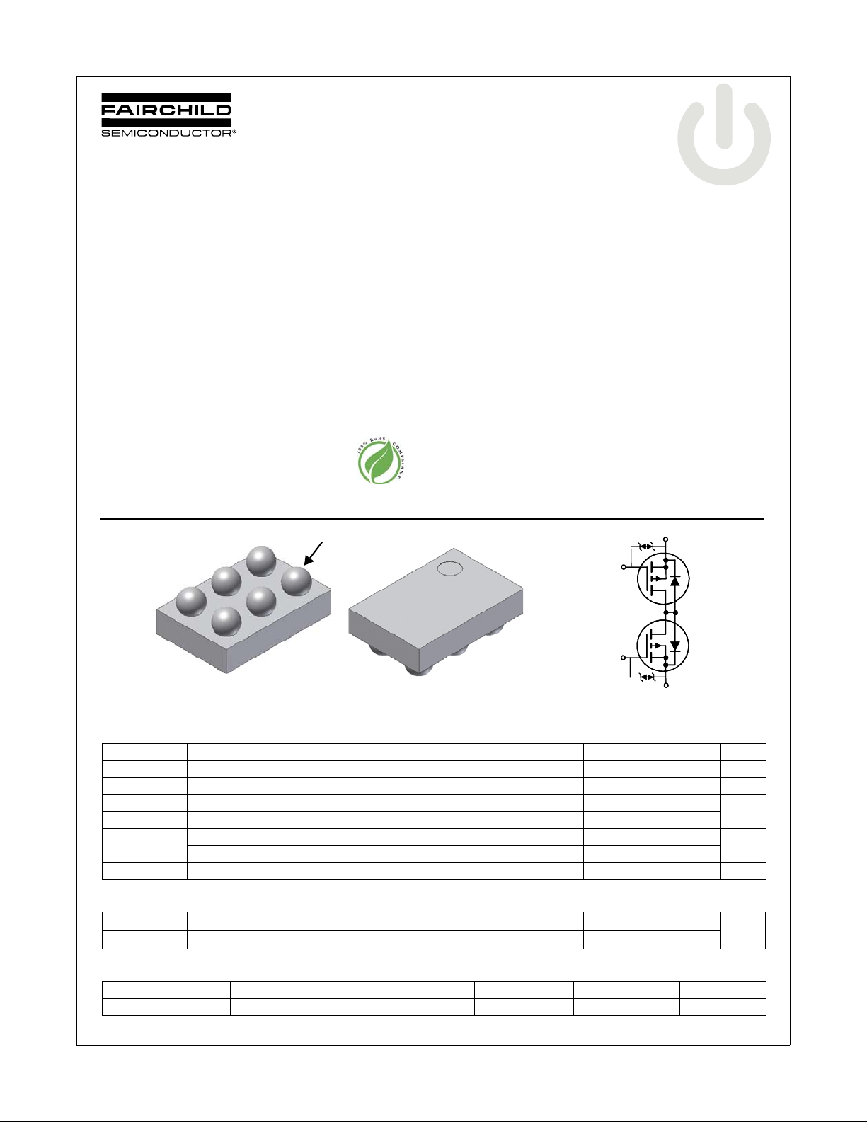
PIN1
= –1A
= –1A
= –1A
= –1A
General Description
This device is designed specifically as a single package solution
for the battery charge switch in cellular handset and other
ultra-portable applications. It features two common drain
P-channel MOSFETs, which enables bidirectional current flow,
on Fairchild’s advanced 1.5V PowerTrench
of the art “low pitch” WL-CSP packaging process, the
FDZ1905PZ minimizes both PCB space and
advanced WL-CSP MOSFET embodies a breakthrough in
packaging technology which enables the device to combine
excellent thermal transfer characteristics, ultra-low profile
packaging, low gate charge, and low
r
S1S2(on)
Applications
Battery management
Load switch
Battery protection
G1
®
process with state
r
. This
S1S2(on)
.
S1
tm
®
WL-CSP MOSFET
BOTTOM
MOSFET Maximum Ratings T
Symbol Parameter Ratings Units
V
S1S2
V
GS
I
S1S2
P
D
, T
T
J
STG
Thermal Characteristics
R
θJA
R
θJA
Package Marking and Ordering Information
Device Marking Device Package Reel Size Tape Width Quantity
©2008 Fairchild Semiconductor Corporation
FDZ1905PZ Rev.B
Source1 to Source2 Voltage –20 V
Gate to Source Voltage ±8 V
Source1 to Source2 Current -Continuous TA = 25°C (Note 1a) –3
-Pulsed –15
Power Dissipation (Steady State) TA = 25°C (Note 1a) 1.5
Power Dissipation T
Operating and Storage Junction Temperature Range –55 to +150 °C
Thermal Resistance, Junction to Ambient (Note 1a) 83
Thermal Resistance, Junction to Ambient (Note 1b) 140
5 FDZ1905PZ WL-CSP 1.0X1.5 7’’ 8mm 5000 units
TOP
= 25°C unless otherwise noted
A
= 25°C (Note 1b) 0.9
A
1
G2
S2
A
W
°C/W
www.fairchildsemi.com

FDZ1905PZ Common Drain P-Channel 1.5V PowerTrench
Electrical Characteristics T
= 25°C unless otherwise noted
J
Symbol Parameter Test Conditions Min Typ Max Units
Off Characteristics
I
S1S2
I
GSS
On Characteristics
V
GS(th)
r
S1S2(on)
g
FS
Switching Characteristics
t
d(on)
t
r
t
d(off)
t
f
Notes:
is determined with the device mounted on a 1in2 pad 2 oz copper pad on a 1.5 x 1.5 in. board of FR- 4 mat erial . R
1. R
θJA
the user's board design.
Zero Gate Voltage Source1 to Source2
Current
Gate Body Leakage Current VGS = ±8V, V
V
S1S2
= –16V, V
S1S2
= 0V –1 µA
GS
= 0V ±10 uA
(Note 2)
Gate to Source Threshold Voltage VGS = V
VGS = –4.5V, I
VGS = –2.5V, I
Static Source1 to Source2 On Resistance
VGS = –1.8V, I
VGS = –1.5V, I
VGS = –4.5V, I
TJ = 125°C
Forward Transconductance V
S1S2
, I
S1S2
= –5V, I
= -250µA –0.4 –0.7 –1.0 V
S1S2
= –1A 99 126
S1S2
= –1A 112 141
S1S2
= –1A 132 198
S1S2
= –1A 164 303
S1S2
= –1A,
S1S2
= –1A 8 S
S1S2
135 195
(Note 2)
Turn-On Delay Time
Rise Time 36 58 ns
Turn-Off Delay Time 143 229 ns
V
= –10V, I
S1S2
VGS = –4.5V, R
S1S2
GEN
= –1A
= 6Ω
Fall Time 182 291 ns
a. 83°C/W when mounted on a
2
pad of 2 oz copper
1 in
θJC
12 22 ns
is guaranteed by design while R
b.140°C/W when mounted on a
minimum pad of 2 oz copper
is determined by
θCA
mΩ
®
WL-CSP MOSFET
2. Pulse Test: Pulse Width < 300ms, Duty cycle < 2.0%.
3. The diode connected between the gate and source serves only protection against ESD. No gate overvo l tag e ra ti ng is im p lie d.
FDZ1905PZ Rev.B
2
www.fairchildsemi.com
 Loading...