tm
FDY6342L
Integrated Load Switch
FDY6342L Integrated Load Switch
October 2008
Features
Max r
Max r
Max r
Max r
Control MOSFET (Q1) includes Zener protection for ESD
ruggedness (>4 kV Human body model)
High performance trench technology for extremely low r
Compact industry standard SC89-6 surface mount package
RoHS Compliant
= 0.5 Ω at VGS = 4.5 V, ID = –0.83 A
DS(on)
= 0.7 Ω at VGS = 2.5 V, ID = –0.70 A
DS(on)
= 1.2 Ω at VGS = 1.8 V, ID = –0.43 A
DS(on)
= 1.8 Ω at VGS = 1.5 V, ID = –0.36 A
DS(on)
DS(on)
Q2
6
5
4
1
2
3
SC89-6
Vin,R1
ON/OFF
R1,C1
4
5
6
General Description
This device is particularly suited for compact power
management in portable electronic equipment where 2.5 V to
8 V input and 0.83 A output current capability are needed. This
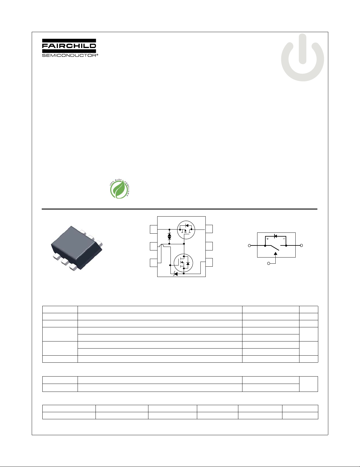
load switch integrates a small N-Channel power MOSFET (Q1)
that drives a large P-Channel power MOSFET (Q2) in one tiny
SC89-6 package.
Applications
Power management
Load switch
Equivalent Circuit
IN
ON/OFF
V
DROP
OUT
Q1
3
2
1
Vout,C1
NC
R2
MOSFET Maximum Ratings T
Symbol Parameter Ratings Units
V
IN
V
ON/OFF
I
Load
P
D
, T
T
J
STG
Thermal Characteristics
R
θJA
R
θJA
Package Marking and Ordering Information
Device Marking Device Package Reel Size Tape Width Quantity
©2008 Fairchild Semiconductor Corporation
FDY6342L Rev.B1
Gate to Source Voltage (Q2) ±8 V
Gate to Source Voltage (Q1) –0.5 to 8 V
Load Current -Continuous (Note 2) –0.83
-Pulsed (Note 2) –1.0
Power Dissipation (Note 1a) 0.625
Power Dissipation (Note 1b) 0.446
Operating and Storage Junction Temperature Range –55 to +150 °C
Thermal Resistance, Junction to Ambient (Note 1a) 200
Thermal Resistance, Junction to Ambient (Note 1b) 280
H FDY6342L SC89-6 7 ’’ 8 mm 3000 units
See Application Circuit
= 25 °C unless otherwise noted
A
1
A
W
°C/W
www.fairchildsemi.com

FDY6342L Integrated Load Switch
Electrical Characteristics T
= 25 °C unless otherwise noted
J
Symbol Parameter Test Conditions Min Typ Max Units
Off Characteristics
BV
I
Load
I
FL
I
RL
IN
VIN Breakdown Voltage ID = –250 µA, V
Zero Gate Voltage Drain Current VIN = –6.4 V, V
Leakage Current, Forward VIN = 8 V, V
Leakage Current, Reverse VIN = –8 V, V
On Characteristics
V
ON/OFF(th)
r
DS(on)
Gate Threshold Voltage VIN = V
Static Drain to Source On Resistance (Q2)
Static Drain to Source On Resistance (Q1)
(note 2)
ON/OFF
ON/OFF
, ID = –250 µA 0.65 0.85 1.5 V
ON/OFF
= 4.5 V, ID = –0.83 A 0.28 0.5
V
IN
V
= 2.5 V, ID = –0.70 A 0.35 0.7
IN
= 1.8 V, ID = –0.43 A 0.45 1.2
V
IN
= 1.5 V, ID = –0.36 A 0.57 1.8
V
IN
V
= 4.5 V, ID = 0.4 A 2.9 4.0
IN
= 2.7 V, ID = 0.2 A 3.5 5.0
V
IN
= 0 V 8 V
ON/OFF
= 0 V –1 µA
ON/OFF
= 0 V 10 µA
= 0 V –10 µA
Drain-Source Diode Characteristics
I
S
V
SD
NOTES:
1. R
θJA
the user's board design.
Maximum Continuous Drain to Source Diode Forward Current –0.25 V
Source to Drain Diode Forward Voltage V
is determined with the device mounted on a 1 in2 pad 2 oz copper pad on a 1.5 x 1.5 in. board of FR-4 material. R
= 0 V, IS = –0.25 A (Note 2) –0.8 –1.2 V
ON/OFF
is guaranteed by design while R
θJC
θJA
is determined by
Ω
Ω
a)200 oC/W when mounted on
a 1 in2 pad of 2 oz copper.
2. Pulse Test: Pulse Width < 300 µs, Duty cycle < 2.0%.
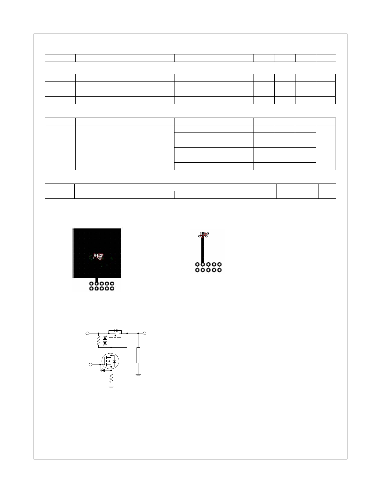
FDY6342L Load Switch Application circuit
Q2
IN
R1
Q1
ON/OFF
R2
External Component Recommendation:
For additional in-rush current c ontrol, R2 and C1 can be added. For more information, see application note AN1030
OUT
C1
LOAD
b)280 oC/W when mounted on a
minimum pad of 2 oz copper.
©2008 Fairchild Semiconductor Corporation
FDY6342L Rev.B1
2
www.fairchildsemi.com
 Loading...