

Fairchild FDY102PZ service manual
t
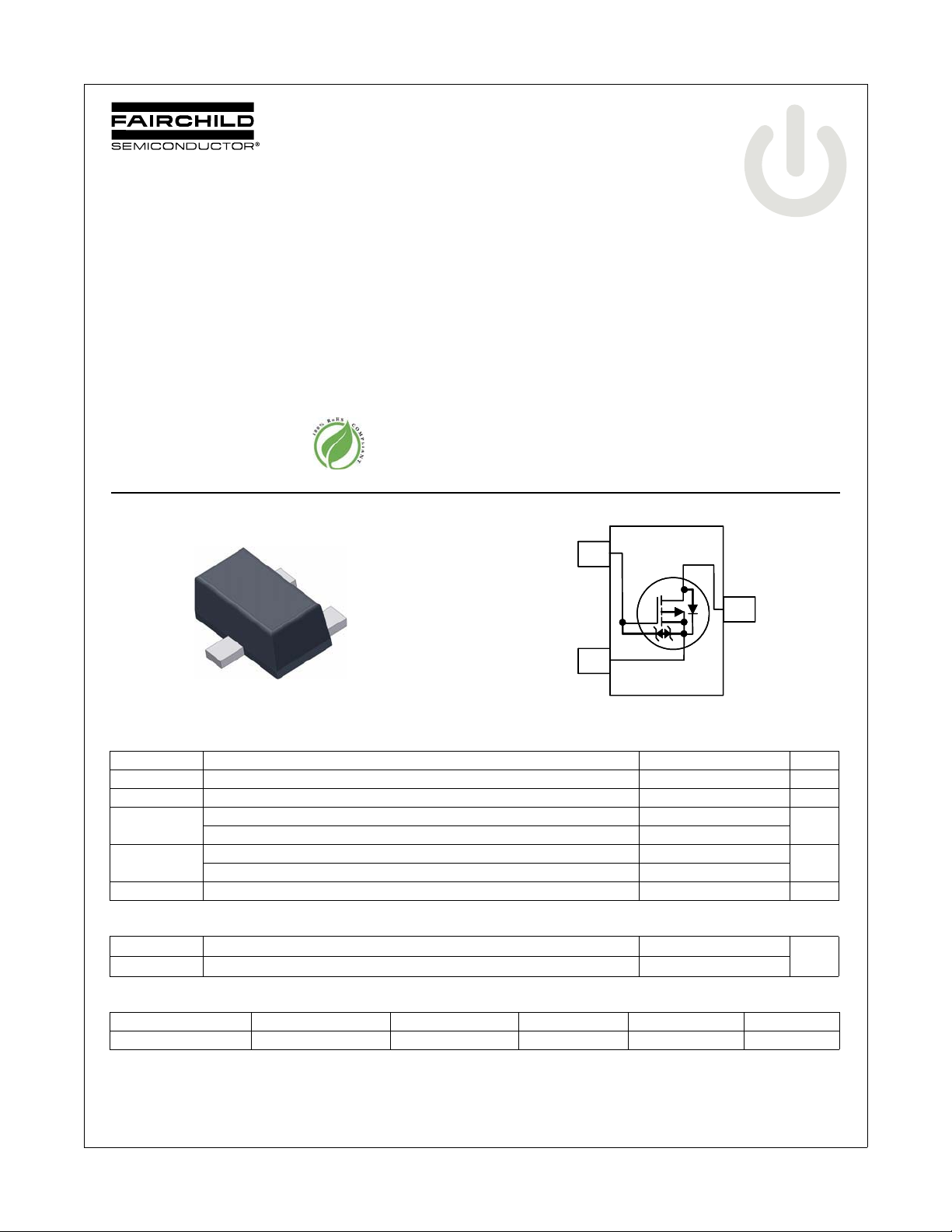
FDY102PZ
Single P-Channel (–1.5 V) Specified PowerTrench®MOSFET
–20 V, –0.83 A, 0.5 :
Features
Max r
Max r
Max r
Max r
HBM ESD protection level = 1400 V (Note 3)
RoHS Compliant
= 0.5 : at VGS = –4.5 V, ID = –0.83 A
DS(on)
= 0.7 : at VGS = –2.5 V, ID = –0.70 A
DS(on)
= 1.2 : at VGS = –1.8 V, ID = –0.43 A
DS(on)
= 1.8 : at VGS = –1.5 V, ID = –0.36 A
DS(on)
General Description
This Single P-Channel MOSFET has been designed using
Fairchild Semiconductor’s advanced Power Trench process to
optimize the r
DS(on)@VGS
= –1.5 V.
Application
Li-Ion Battery Pack
FDY102PZ Single P-Channel (–1.5 V) Specified PowerTrench
February 2010
m
1
S
G
D
MOSFET Maximum Ratings T
Symbol Parameter Ratings Units
V
DS
V
GS
I
D
P
D
, T
T
J
STG
Drain to Source Voltage –20 V
Gate to Source Voltage ±8 V
Drain Current -Continuous (Note 1a) –0.83
-Pulsed –1.0
Power Dissipation (Note 1a) 0.625
Power Dissipation (Note 1b) 0.446
Operating and Storage Junction Temperature Range –55 to +150 °C
SC89-3
= 25 °C unless otherwise noted
A
G
D
3
S
2
Thermal Characteristics
R
TJA
R
TJA
Thermal Resistance, Junction to Ambient (Note 1a) 200
Thermal Resistance, Junction to Ambient (Note 1b) 280
Package Marking and Ordering Information
®
MOSFET
A
W
°C/W
Device Marking Device Package Reel Size Tape Width Quantity
E FDY102PZ SC89-3 7 ” 8 mm 3000 units
©2010 Fairchild Semiconductor Corporation
FDY102PZ Rev.B2
1
www.fairchildsemi.com
FDY102PZ Single P-Channel (–1.5 V) Specified PowerTrench
Electrical Characteristics T
= 25 °C unless otherwise noted
J
Symbol Parameter Test Conditions Min Typ Max Units
Off Characteristics
BV
DSS
'BV
DSS
'T
J
I
DSS
I
GSS
On Characteristics
V
GS(th)
'V
GS(th)
'T
J
r
DS(on)
g
FS
Drain to Source Breakdown Voltage ID = –250 PA, VGS = 0 V –20 V
Breakdown Voltage Temperature
Coefficient
I
= –250 PA, referenced to 25 °C -11 mV/°C
D
Zero Gate Voltage Drain Current VDS = –16 V, VGS= 0 V –1 PA
Gate to Source Leakage Current VGS = ±8 V, V
= 0 V ±10 PA
DS
(Note 2)
Gate to Source Threshold Voltage VGS = VDS, ID = –250 PA –0.4 –0.7 –1.0 V
Gate to Source Threshold Voltage
Temperature Coefficient
Static Drain to Source On-Resistance
I
= –250 PA, referenced to 25 °C 3 mV/°C
D
V
= –4.5 V, ID = –0.83 A 0.28 0.5
GS
= –2.5 V, ID = –0.70 A 0.36 0.7
V
GS
= –1.8 V, ID = –0.43 A 0.47 1.2
V
GS
= –1.5 V, ID = –0.36 A 0.62 1.8
V
GS
= –4.5 V, ID = –0.83 A,
V
GS
T
=125 °C
J
0.39 0.85
Forward Transconductance VDD = –5 V, ID = –0.83 A 2 S
Dynamic Characteristics
C
iss
C
oss
C
rss
Input Capacitance
Output Capacitance 23 35 pF
Reverse Transfer Capacitance 18 30 pF
= –10 V, VGS = 0 V,
V
DS
f = 1 MHz
100 135 pF
:
Switching Characteristics
t
d(on)
t
r
t
d(off)
t
f
Q
Q
Q
g
gs
gd
Turn-On Dela y Time
Rise Time 2.9 10 ns
Turn-Off Delay Time 23 37 ns
Fall Time 13 23 ns
Total Gate Charge
Gate to Source Charge 0.3 nC
Gate to Drain “Miller” Charge 0.6 nC
(Note 2)
= –10 V, ID = –0.83 A
V
DD
V
= –4.5 V, R
GS
= –10 V, ID = –0.83 A
V
DD
V
= –4.5 V
GS
GEN
Drain-Source Diode Characteristics and Maximum Rating
I
S
V
SD
t
rr
Q
rr
Notes:
1. R
is determined with the device mounted on a 1 in2 oz. copper pad on a 1.5 x 1.5 in. board of FR-4 material. R
TJA
user's board design.
Maximum Continuous Drain-Source Diode Forward Current –0.52 A
Source to Drain Diode Forward Voltage VGS= 0 V, IS= –0.52 A (Note 2) –1.0 –1.2 V
Reverse Recovery Time
Reverse Recovery Charge 3.8 10 nC
a) 200 oC/W when mounted on
2
pad of 2 oz copper.
a 1 in
= –0.83 A, dIF/dt = 100 A/Ps
I
F
= 6 :
3.5 10 ns
18 31 ns
is guaranteed by design while R
TJC
o
b) 280
C/W when mounted on a
minimum pad of 2 oz copper.
2.2 3.1 nC
is determined by the
TJA
®
MOSFET
2. Pulse Test : Pulse Width < 300 us, Duty Cycle < 2.0%
3: The diode connected between the gate and source serves only as protection against ESD. No gate overvoltage rating is implied.
©2010 Fairchild Semiconductor Corporation
FDY102PZ Rev.B2
2
www.fairchildsemi.com
FDY102PZ Single P-Channel (–1.5 V) Specified PowerTrench
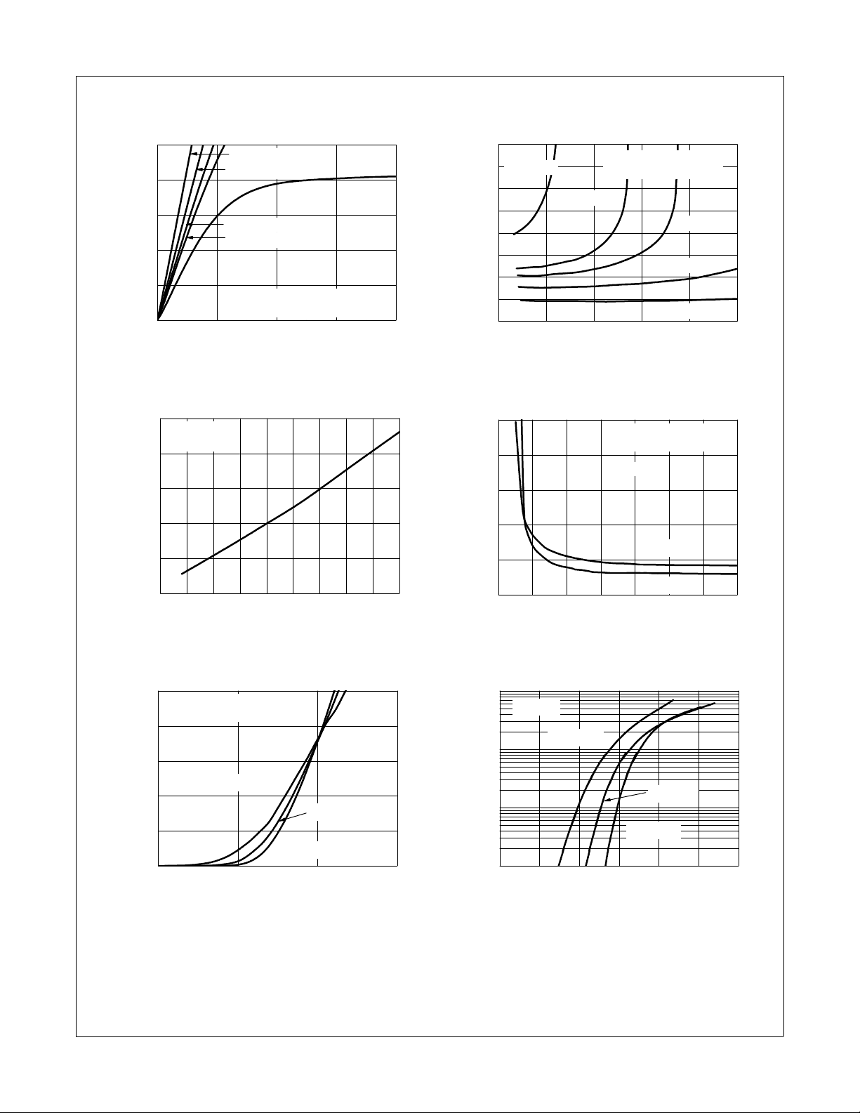
Typical Characteristics T
1.0
0.8
0.6
0.4
, DRAIN CURRENT (A)
D
-I
0.2
0.0
0.00.51.01.52.0
-V
Figure 1.
1.6
ID = -0.83 A
V
= -4.5 V
GS
1.4
1.2
1.0
NORMALIZED
0.8
DRAIN TO SOURCE ON-RESISTANCE
0.6
-75 -50 -25 0 25 50 75 100 125 150
F i g u r e 3 . N o r m a l i z e d O n R e s i s t a n c e
vs Junction Temperature
VGS = -4.5 V
VGS = -2.5 V
VGS = -2.0 V
VGS = -1.8 V
PULSE DURATION = 80 Ps
DUTY CYCLE = 0.5% MAX
, DRAIN TO SOURCE VOLTAGE (V)
DS
On Region Characteristics Figure 2.
T
, JUNCTION TEMPERATURE (
J
= 25 °C unless otherwise noted
J
VGS = -1.5 V
o
C)
4.5
4.0
3.5
VGS = -1.5 V
PULSE DURATION = 80 Ps
DUTY CYCLE = 0.5%MAX
VGS = -1.8 V
3.0
VGS= -2.0V
VGS = -2.5 V
NORMALIZED
2.5
2.0
1.5
1.0
DRAIN TO SOURCE ON-RESISTANCE
0.5
0.00.51.01.52.02.5
-I
, DRAIN CURRENT (A)
D
V
GS
=-4.5 V
N o r m a l i z e d O n - R e s i s t a n c e
vs Drain Current and Gate Voltage
2.0
(:)
1.6
1.2
DRAIN TO
,
0.8
DS(on)
r
0.4
SOURCE ON-RESISTANCE
0.0
1.0 1.5 2.0 2.5 3.0 3.5 4.0 4.5
-V
, GATE TO SOURCE VOLTAGE (V)
GS
Figure 4.
O n - R es i s t a n c e vs G a t e t o
PULSE DURATION = 80 Ps
DUTY CYCLE = 0.5% MAX
ID= -0.415 A
TJ= 125 oC
TJ= 25 oC
Source Voltage
®
MOSFET
1.0
PULSE DURATION = 80 P s
DUTY CYCLE = 0.5% MAX
0.8
V
= -5 V
DS
0.6
0.4
TJ = 125 oC
, DRAIN CURRENT (A)
D
-I
0.2
0.0
0.51.01.52.0
-VGS, GATE TO SOURCE VOLTAGE (V)
Figure 5. Transfer Characteristics
©2010 Fairchild Semiconductor Corporation
FDY102PZ Rev.B2
TJ = 25 oC
TJ = -55 oC
1
V
= 0 V
GS
0.1
TJ= 125 oC
TJ = 25 oC
0.01
, REVERSE DRAIN CURRENT (A)
S
-I
0.001
0.0 0.2 0.4 0.6 0.8 1.0 1.2
-VSD, BODY DIODE FORWARD VOLTAGE (V)
Figure 6.
S o u r ce t o D r a i n Di o d e
TJ = -55 oC
Forward Voltage vs Source Current
3
www.fairchildsemi.com
 Loading...