

Fairchild FDT86256 service manual
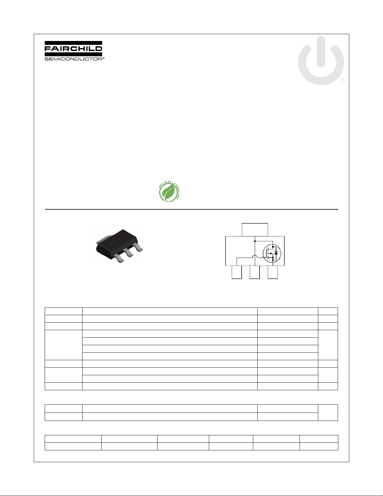
FDT86256
G
D
S
D
SOT-223
SG
D
D
N-Channel PowerTrench® MOSFET
150 V, 1.2 A, 845 mΩ
Features
Max r
Max r
Very low Qg and Qgd compared to competing trench
technologies
= 845 mΩ at V
DS(on)
= 1280 mΩ at V
DS(on)
= 10 V, ID = 1.2 A
GS
= 6.0 V, ID = 1.0 A
GS
General Description
This N-Channel MOSFET is produced using Fairchild
Semiconductor’s advanced PowerTrench
been especially tailored to minimize the on-state resistance and
switching loss. G-S zener has been added to enhance ESD
voltage level.
August 2011
®
process that has
FDT86256 N-Channel PowerTrench
Fast switching speed
100% UIL Tested
RoHS Compliant
MOSFET Maximum Ratings T
Symbol Parameter Ratings Units
V
DS
V
GS
I
D
E
AS
P
D
, T
T
J
STG
Drain to Source Voltage 150 V
Gate to Source Voltage ±20 V
Drain Current -Continuous (Package limited) TC = 25 °C 3
-Continuous (Silicon limited) T
-Continuous T
-Pulsed 2
Single Pulse Avalanche Energy (Note 3) 1 mJ
Power Dissipation TC = 25 °C 10
Power Dissipation T
Operating and Storage Junction Temperature Range -55 to +150 °C
= 25 °C unless otherwise noted
A
Applications
DC-DC conversion
Inverter
Synchronous Rectifier
= 25 °C 2.5
C
= 25 °C (Note 1a) 1.2
A
= 25 °C (Note 1a) 2.3
A
Thermal Characteristics
®
MOSFET
A
W
R
θJC
R
θJA
Thermal Resistance, Junction to Case 12
Thermal Resistance, Junction to Ambient (Note 1a) 55
°C/W
Package Marking and Ordering Information
Device Marking Device Package Reel Size Tape Width Quantity
©2011 Fairchild Semiconductor Corporation 1 www.fairchildsemi.com
FDT86256 Rev. C
86256 FDT86256 SOT-223 13 ’’ 12 mm 2500 units
FDT86256 N-Channel PowerTrench
Electrical Characteristics T
= 25 °C unless otherwise noted
J
Symbol Parameter Test Conditions Min Typ Max Units
Off Characteristics
BV
ΔBV
ΔT
I
DSS
I
GSS
DSS
DSS
J
Drain to Source Breakdown Voltage ID = 250 μA, VGS = 0 V 150 V
Breakdown Voltage Temperature
Coefficient
Zero Gate Voltage Drain Current VDS = 120 V, V
Gate to Source Leakage Current VGS = ±20 V, V
I
= 250 μA, referenced to 25 °C 100 mV/°C
D
= 0 V 1 μA
GS
= 0 V ±10 μA
DS
On Characteristics
V
GS(th)
ΔV
ΔT
r
DS(on)
g
FS
GS(th)
J
Gate to Source Threshold Voltage VGS = VDS, ID = 250 μA23.54V
Gate to Source Threshold Voltage
Temperature Coefficient
Static Drain to Source On Resistance
I
= 250 μA, referenced to 25 °C -8 mV/°C
D
V
= 10 V, ID = 1.2 A 695 845
GS
= 6 V, ID = 1.0 A 912 1280
GS
= 10 V, ID = 1.2 A, TJ = 125 °C 1298 1367
V
GS
Forward Transconductance VDS = 5 V, ID = 1.2 A 0.3 S
Dynamic Characteristics
C
iss
C
oss
C
rss
R
g
Input Capacitance
Output Capacitance 8 11 pF
Reverse Transfer Capacitance 1 1.4 pF
= 75 V, VGS = 0 V,
V
DS
f = 1MHz
Gate Resistance 1.3 Ω
55 73 pF
Switching Characteristics
t
d(on)
t
r
t
d(off)
t
f
Q
g(TOT)
Q
g(TOT)
Q
gs
Q
gd
Turn-On Delay Time
Rise Time 1.7 10 ns
Turn-Off Delay Time 4.8 10 ns
= 75 V, ID = 1.2 A,
V
DD
V
= 10 V, R
GS
GEN
= 6 Ω
Fall Time 2.6 10 ns
Total Gate Charge V
Total Gate Charge V
Gate to Source Charge 0.4 nC
= 0 V to 10 V
GS
= 0 V to 6 V 0.8 1.0
GS
V
DD
I
= 1.2 A
D
= 75 V,
Gate to Drain “Miller” Charge 0.3 nC
2.7 10 ns
1.2 2.0 nC
mΩV
®
MOSFET
Drain-Source Diode Characteristics
V
= 0 V, IS = 1.2 A (Note 2) 0.9 1.3
V
SD
t
rr
Q
rr
NOTES:
1. R
is determined with the device mount ed on a 1 in2 pad 2 oz copper pad on a 1.5 x 1. 5 in. bo ard of FR-4 mater ial. R
θJA
the user's board design.
2. Pulse Test: Pulse Width < 300 μs, Duty cycle < 2.0 %.
3. Starting T
4. The diode connected between gate and source serves only as protection against ESD. No gate overvoltage rating is implied.
©2011 Fairchild Semiconductor Corporation 2 www.fairchildsemi.com
FDT86256 Rev. C
Source to Drain Diode Forward Voltage
Reverse Recovery Time
Reverse Recovery Charge 24 38 nC
a)
= 25 °C, L = 3 mH, IAS = 1 A, V
J
= 150 V, VGS = 10 V.
DD
GS
= 0 V, IS = 1.0 A (Note 2) 0.8 1.3
V
GS
= 1.2 A, di/dt = 100 A/μs
I
F
55 °C/W when mounted on a
2
1 in
pad of 2 oz copper
47 75 ns
is guaranteed by design while R
θJC
118 °C/W when mounted on
b)
a minimum pad of 2 oz copper
is determined by
θCA
V
 Loading...