

Fairchild FDS8984 service manual
tm
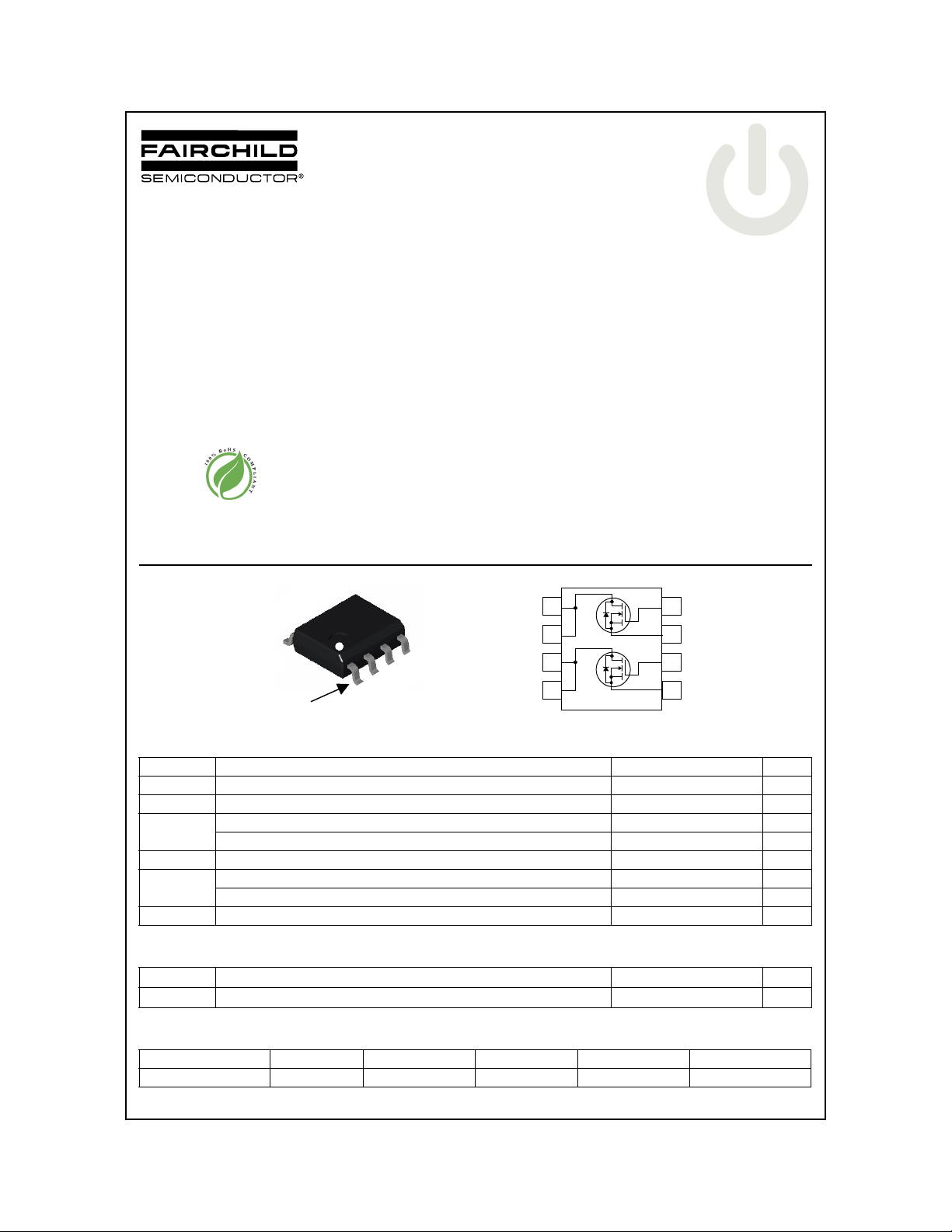
FDS8984
N-Channel PowerTrench® MOSFET
30V, 7A, 23mΩ
FDS8984 N-Channel PowerTrench
May 2007
General Description
This N-Channel MOSFET has been designed specifically to
improve the overall efficiency of DC/DC converters using
either synchronous or conventional switching PWM
controllers. It has been optimized for low gate charge, low
r
and fast switching speed.
DS(ON)
D2
D
D2
D
D1
D
D1
D
SO-8
Pin 1
SO-8
S1
MOSFET Maximum Ratings T
Symbol Parameter Ratings Units
V
DS
V
GS
I
D
E
AS
P
D
, T
T
J
STG
Drain to Source Voltage 30 V
Gate to Source Voltage ±20 V
Drain Current Continuous (Note 1a) 7 A
Pulsed 30 A
Single Pulse Avalache Energy (Note 2) 32 mJ
Power Dissipation for Single Operation 1.6 W
Derate above 25°C 13 mW/°C
Operating and Storage Temperature -55 to 150 °C
G2
S2
G
G1
S
S
S
= 25°C unless otherwise noted
A
Features
Max r
Max r
Low gate charge
100% R
RoHS Compliant
= 23mΩ, V
DS(on)
= 30mΩ, V
DS(on)
tested
G
5
6
7
8
Q2
Q1
= 10V, ID = 7A
GS
= 4.5V, ID = 6A
GS
4
3
2
1
®
MOSFET
Thermal Characteristics
R
θJA
R
θJC
Thermal Resistance, Junction-to-Ambient (Note 1a) 78 °C/W
Thermal Resistance, Junction-to-Case (Note 1) 40 °C/W
Package Marking and Ordering Information
Device Marking Device Package Reel Size Tape Width Quantity
FDS8984 FDS8984 SO-8 330mm 12mm 2500 units
©2007 Fairchild Semiconductor Corporation
FDS8984 Rev. A1
www.fairchildsemi.com1
FDS8984 N-Channel PowerTrench
Electrical Characteristics T
= 25°C unless otherwise noted
J
Symbol Parameter Test Conditions Min Typ Max Units
Off Characteristics
BV
DSS
∆BV
DSS
∆T
J
I
DSS
I
GSS
On Characteristics
V
GS(th)
∆V
GS(th)
∆T
J
r
DS(on)
Drain to Source Breakdown Voltage ID = 250µA, VGS = 0V 30 V
Breakdown Voltage Temperature
Coefficient
Zero Gate Voltage Drain Current
ID = 250µA, referenced to
25°C
V
= 24V
DS
V
= 0V
GS
= 125°C 250
T
J
23 mV/°C
1
Gate to Source Leakage Current VGS = ±20V,VDS = 0V ±100 nA
(Note 3)
Gate to Source Threshold Voltage VDS = VGS, ID = 250µA 1.2 1.7 2.5 V
Gate to Source Threshold Voltage
Temperature Coefficient
Drain to Source On Resistance
ID = 250µA, referenced to
25°C
= 10V, ID = 7A 19 23
V
GS
V
= 4.5V, ID = 6A 24 30
GS
= 10V, ID = 7A,
V
GS
T
= 125°C
J
- 4.3 mV/°C
26 32
Dynamic Characteristics
C
iss
C
oss
C
rss
R
G
Input Capacitance
Output Capacitance 100 135 pF
Reverse Transfer Capacitance 65 100 pF
= 15V, VGS = 0V,
V
DS
f = 1.0MHz
Gate Resistance f = 1MHz 0.9 1.6 Ω
475 635 pF
µA
mΩ
®
MOSFET
Switching Characteristics
t
d(on)
t
r
t
d(off)
t
f
Q
Q
Q
Q
g
g
gs
gd
Turn-On Delay Time
Rise Time 918ns
Turn-Off Delay Time 42 68 ns
Fall Time 21 34 ns
Total Gate Charge
Total Gate Charge
Gate to Source Gate Charge 1.5 nC
Gate to Drain “Miller” Charge 2.0 nC
(Note 3)
= 15V, ID = 7A
V
DD
V
= 10V, R
GS
V
= 15V, VGS = 10V,
DS
I
= 7A
D
V
= 15V, VGS = 5V,
DS
I
= 7A
D
GS
510ns
= 33Ω
9.2 13 nC
5.0 7 nC
Drain-Source Diode Characteristics
I
= 7A 0.9 1.25 V
V
SD
t
rr
Q
rr
Notes:
1: R
θJA
the drain pins. R
Source to Drain Diode Voltage
Diode Reverse Recovery Time
Diode Reverse Recovery Charge 20 nC
is the sum of the junction-to-case and case-to-ambient thermal resistance where the case thermal reference is defined as the solder mounting surface of
is guaranteed by design while R
θJC
a) 78°C/W when
mounted on a 0.5in
pad of 2 oz copper
is determined by the user’s board design.
θCA
2
SD
= 2.1A 0.8 1.0 V
I
SD
I
= 7A, di/dt = 100A/µs
F
b) 125°C/W when
mounted on a 0.02 in
pad of oz copper
2
c) 135°C/W when
mounted on a
minimun pad
33 ns
Scale 1 : 1 on letter size paper
2: Starting TJ = 25°C, L = 1mH, IAS = 8A, VDD = 27V, V
3: Pulse Test:Pulse Width <300µs, Duty Cycle <2%.
FDS8984 Rev. A1
GS
= 10V.
www.fairchildsemi.com2
 Loading...