

Page 1
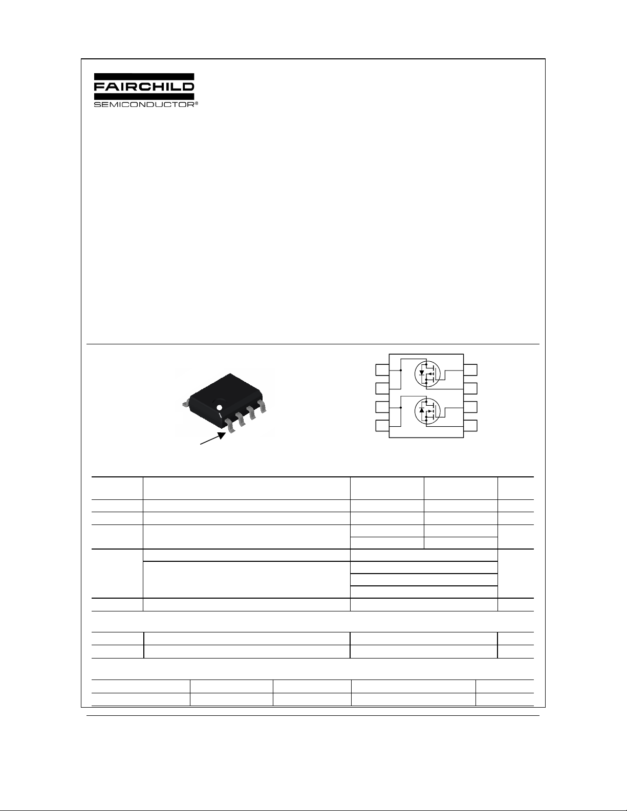
FDS8958A
Dual N & P-Channel PowerTrench
MOSFET
FDS8958A
January 2002
General Description
These dual N- and P-Channel enhancement mode
power field effect transistors are produced using
Fairchild Semiconductor’s advanced PowerTrench
process that has been especially tailored to minimize
on-state ressitance and yet maintain superior switching
performance.
These devices are well suited for low voltage and
battery powered applications where low in-line power
loss and fast switching are required.
D2
D
D2
D
D1
D
D1
D
SO-8
Pin 1
SO-8
S1
Absolute Maximum Ratings T
G2
S2
G
G1
S
S
S
= 25°C unless otherwise noted
A
Features
• Q1: N-Channel
7.0A, 30V R
R
• Q2: P-Channel
-5A, -30V R
R
• Fast switching speed
• High power and handling capability in a widely
used surface mount package
5
6
7
8
= 0.028Ω @ VGS = 10V
DS(on)
= 0.040Ω @ VGS = 4.5V
DS(on)
= 0.052Ω @ VGS = -10V
DS(on)
= 0.080Ω @ VGS = -4.5V
DS(on)
Q2
Q1
4
3
2
1
Symbol Parameter Q1 Q2 Units
V
Drain-Source Voltage 30 30 V
DSS
V
Gate-Source Voltage
GSS
ID Drain Current - Continuous (Note 1a) 7 -5 A
- Pulsed 20 -20
PD Power Dissipation for Dual Operation 2 W
Power Dissipation for Single Operation (Note 1a) 1.6
TJ, T
STG
Operating and Storage Junction Temperature Range -55 to +150
(Note 1b)
(Note 1c)
±20 ±20
1
0.9
V
°C
Thermal Characteristics
R
θJA
R
θJC
Thermal Resistance, Junction-to-Ambient
Thermal Resistance, Junction-to-Case
(Note 1a) 78
(Note 1) 40
°C/W
°C/W
Package Marking and Ordering Information
Device Marking Device Reel Size Tape width Quantity
FDS8958A FDS8958A 13” 12mm 2500 units
2002 Fairchild Sem iconductor Corporation
FDS8958A Rev D1(W )
Page 2
FDS8958A
Electrical Characteristics T
= 25°C unless otherwise noted
A
Symbol Parameter Test Conditions Type Min Typ Max Units
Off Characteristics
Q1
BV
Drain-Source Breakdown
DSS
Voltage
∆BVDSS
∆T
I
Zero Gate Voltage Drain
DSS
Breakdown Voltage
Temperature Coefficient
J
Current
I
Gate-Body Leakage, Forward VGS = 20 V, VDS = 0 V All 100 nA
GSSF
I
Gate-Body Leakage, Reverse VGS = -20 V, VDS = 0 V All -100 nA
GSSR
V
= 0 V, ID = 250 µA
GS
= 0 V, ID = -250 µA
V
GS
= 250 µA, Referenced to 25°C
I
D
= -250 µA, Referenced to 25°C
I
D
VDS = 24 V, VGS = 0 V
= -24 V, VGS = 0 V
V
DS
Q2
Q1
Q2
Q1
Q2
30
-30
V
25
mV/°C
-22
1
-1
On Characteristics (Note 2)
V
Gate Threshold Voltage
GS(th)
∆VGS(th)
∆TJ
R
DS(on)
Gate Threshold Voltage
Temperature Coefficient
Static Drain-Source
On-Resistance
I
On-State Drain Current VGS = 10 V, VDS = 5 V
D(on)
V
= VGS, ID = 250 µA
DS
= VGS, ID = -250 µA
V
DS
= 250 µA, Referenced to 25°C
I
D
= -250 µA, Referenced to 25°C
I
D
VGS = 10 V, ID = 7 A
= 10 V, ID = 7 A, TJ = 125°C
V
GS
= 4.5 V, ID = 6 A
V
GS
V
= -10 V, ID = -5 A
GS
= -10 V, ID = -5 A, TJ = 125°C
V
GS
= -4.5 V, ID = -4 A
V
GS
V
= -10 V, VDS = -5 V
GS
gFS Forward Transconductance VDS = 5 V, ID = 7 A
= -5 V, ID =-5 A
V
DS
Q1
Q2 1 -1
Q1
Q2
Q1 21
Q2 41
Q1
Q2
Q1
Q2
1.6
-1.7 3 -3
-4.3 4
32
27
58
58
20
A
-20
19
11
mV/°C
28
mΩ
42
40
52
78
80
S
Dynamic Characteristics
C
Input Capacitance Q1
iss
C
Output Capacitance Q1
oss
C
Reverse Transfer Capacitance
rss
Q1
= 10 V, VGS = 0 V, f = 1.0 MHz
V
DS
Q2
= -10 V, VGS = 0 V, f = 1.0 MHz
V
DS
Q2
Q2
Q1
Q2
789
690
173
306
66
77
pF
pF
pF
µA
V
FDS8958A Rev D1(W )
Page 3
FDS8958A
Electrical Characteristics (continued) T
Symbol
Parameter
Test Conditions
= 25°C unless otherwise noted
A
Type Min Typ Max Units
Switching Characteristics (Note 2)
t
Turn-On Delay Time
d(on)
tr Turn-On Rise Time
t
Turn-Off Delay Time
d(off)
tf Turn-Off Fall Time
Qg Total Gate Charge
Qgs Gate-Source Charge
Qgd Gate-Drain Charge
Q1
VDD = 10 V, ID = 1 A,
V
= 10V, R
GS
GEN
= 6 Ω
Q2
= -10 V, ID = -1 A,
V
DD
= -10V, R
V
GS
GEN
= 6 Ω
Q1
= 15 V, ID = 7 A, VGS = 10 V
V
DS
Q2
V
= -15 V, ID = -5 A,VGS = -10 V
DS
Q1
Q2
Q1
Q2
Q1
Q2
Q1
Q2
Q1
Q2
Q1
Q2
Q1
Q2
2.2
6.7
13.4
7.5
9.7
19.8
19.4
21.3
35.6
11.8
3.7
12.3
22.2
16
14
2.5
2.2
2.1
1.9
4.4
7.4
Drain–Source Diode Characteristics and Maximum Ratings
IS Maximum Continuous Drain-Source Diode Forward Current Q1
Q2
VSD Drain-Source Diode Forward
Voltage
Notes:
1. R
is the sum of the junction-to-case and case-to-ambient thermal resistance where the case thermal reference is defined as the solder mounting surface of
θJA
the drain pins. R
is guaranteed by design while R
θJC
VGS = 0 V, IS = 1.3 A (Note 2)
VGS = 0 V, IS = -1.3 A (Note 2)
is determined by the user's board design.
θCA
Q1
Q2
1.3
-1.3
0.74
-0.76
1.2
-1.2
ns
15
ns
ns
ns
26
nC
23
nC
nC
A
V
a) 78°/W when
mounted on a
0.5 in2 pad of 2 oz
copper
Scale 1 : 1 on letter size paper
2. Pulse Test: Pulse Width < 300µs, Duty Cycle < 2.0%
b) 125°/W when
mounted on a .02 in2
pad of 2 oz copper
c) 135°/W when mounted on a
mini mum pa d.
FDS8958A Rev D1(W )
Page 4

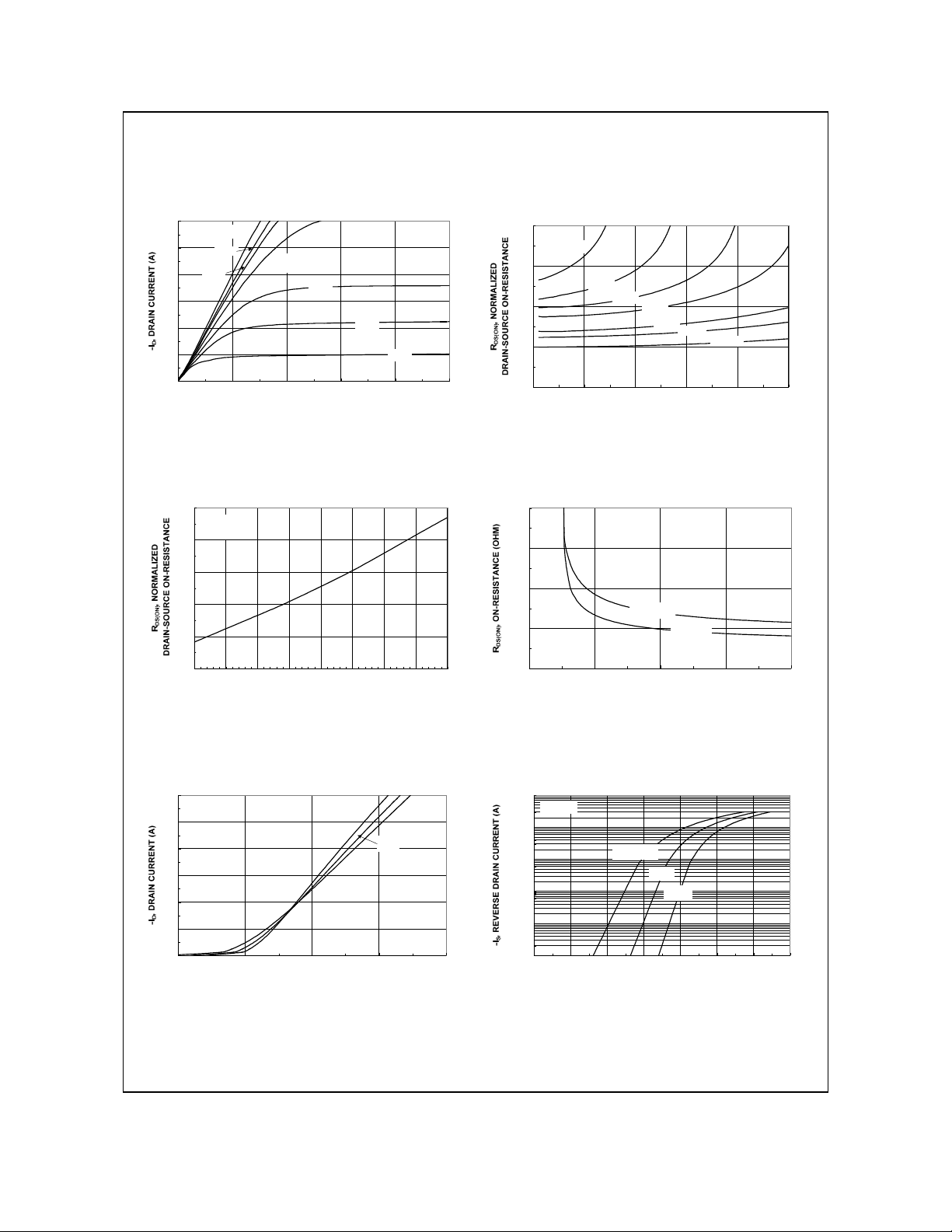
Typical Characteristics: Q1
FDS8958A
30
VGS = 10V
5.0V
20
4.5V
10
, DRAIN CURRENT (A)
D
I
0
012345
7.0V
4.0V
V
DS
3.5V
3.0V
, DRAIN-SOURCE VOL TAGE (V)
2.5V
2.4
VGS = 3.0V
2.2
2.0
1.8
1.6
1.4
1.2
1.0
0.8
0 6 12 18 24 30
3.5V
4.0V
4.5V
, DRAIN CURRENT (A)
I
D
5.0V
6.0V
Figure 1. On-Region Characteristics. Figure 2. On-Resistance Variation with
Drain Current and Gate Voltage.
1.9
ID = 7A
= 10V
V
GS
1.6
1.3
1.0
0.7
0.4
-50 -25 0 25 50 75 100 125 150
, JUNCTION TEM PERATURE (oC)
T
J
0.09
0.08
0.07
0.06
0.05
0.04
0.03
0.02
0.01
TA = 25oC
246810
TA = 125oC
V
, GATE TO SOURCE VOLTAGE (V)
GS
7.0V
10V
ID = 7A
Figure 3. On-Resistance Variation with
Temperature.
30
VDS = 10V
25
20
15
10
, DRAIN CURRENT (A)
D
I
5
0
12345
V
GS
TA = -55oC
125oC
, GATE TO SOURCE VOLTAGE (V)
25oC
Figure 5. Transfer Characteristics. Figure 6. Body Diode Forward Voltage Variation
Figure 4. On-Resistance Variation with
Gate-to-Source Voltage.
100
VGS = 0V
10
1
0.1
0.01
0.001
00.20.40.60.811.21.4
TA = 125oC
25oC
-55oC
V
, BODY DIODE FORWA RD VOLTAGE (V)
SD
with Source Current and Temperature.
FDS8958A Rev D1(W )
Page 5
µ
Typical Characteristics: Q1
FDS8958A
10
ID =7A
8
6
4
2
, GATE-SOURCE VOLTAGE ( V)
GS
V
0
0 4 8 12 16
Q
, GATE CHARGE (nC)
g
VDS = 5V
15V
10V
1200
900
600
300
0
0.0 5.0 10.0 15.0 20.0
C
ISS
C
OSS
C
RSS
V
, DRAIN TO SOURCE VOLTAGE (V)
DS
Figure 7. Gate Charge Characteristics. Figure 8. Capacitance Characteristics.
100
R
LIMIT
DS(ON)
1s
100ms
10ms
1ms
10
1
VGS = 10V
SINGLE PULSE
0.1
= 135oC/W
R
θ
JA
= 25oC
T
0.01
A
0.1 1 10 100
V
DS
10s
DC
, DRAIN-SOURCE VO LTAGE (V)
50
40
30
20
10
0
0.001 0.01 0.1 1 10 100 1000
t
, TIME (sec)
1
SINGLE PULSE
= 135°C/W
R
θ
JA
= 25°C
T
A
f = 1MHz
V
= 0 V
GS
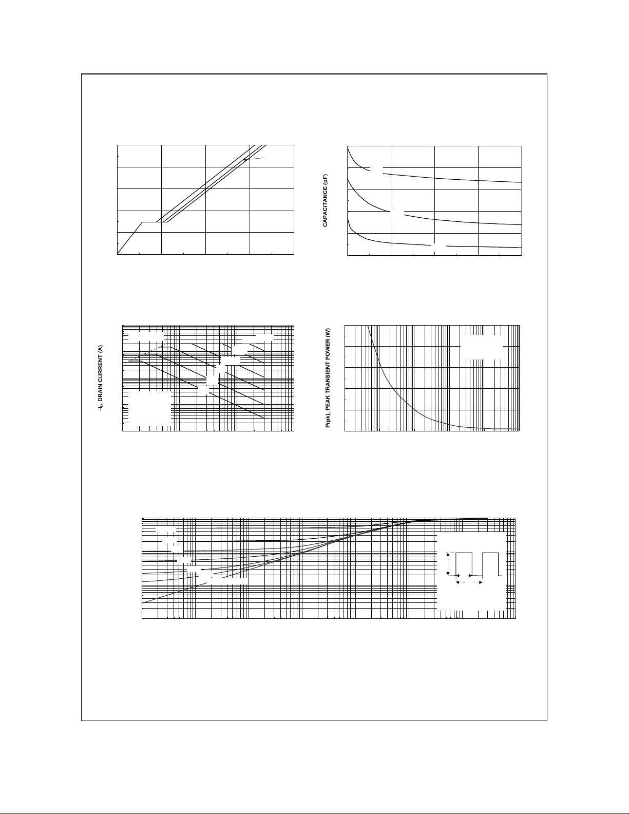
Figure 9. Maximum Safe Operating Area. Figure 10. Single Pulse Maximum
Power Dissipation.
FDS8958A Rev D1(W )
Page 6
Typical Characteristics: Q2
FDS8958A
30
VGS = -10.0V
25
20
15
10
5
0
-
-
012345
-5.0V
-4.0V
, DRAIN TO SOURCE VOLTAGE (V)
-V
DS
-3.5V
-3.0V
2.5
VGS = -3.5V
2
-4.0V
1.5
1
0.5
0 6 12 18 24 30
-4.5V
-5.0V
-6.0V
, DRAIN CURRENT (A)
-I
D
-7.0V
-10.0V
Figure 11. On-Region Characteristics. Figure 12. On-Resistance Variation with
Drain Current and Gate Voltage.
1.6
ID = -5A
V
= -10V
GS
1.4
1.2
1.0
0.8
0.6
-50 -25 0 25 50 75 100 125 150
, JUNCTION TEM PERATURE (oC)
T
J
0.2
0.15
0.1
TA = 125oC
0.05
0
246810
-V
, GATE TO SOURCE VOLTAGE (V)
GS
TA = 25oC
ID = -5A
Figure 13. On-Resistance Variation with
Temperature.
30
VDS = -10V
25
20
15
10
5
0
1.5 2.5 3.5 4.5 5.5
-V
, GATE TO SOURCE VOLTAGE (V)
GS
TA = -55oC
25oC
125oC
Figure 14. On-Resistance Variation with
Gate-to-Source Voltage.
100
VGS = 0V
10
1
0.1
0.01
0.001
0 0.2 0.4 0.6 0.8 1 1.2 1.4
TA = 125oC
25oC
-55oC
-V
BODY DIODE F ORWARD VOLTA GE (V)
SD,
Figure 15. Transfer Characteristics. Figure 16. Body Diode Forward Voltage Variation
with Source Current and Temperature.
FDS8958A Rev D1(W )
Page 7
µ
)
Typical Characteristics: Q2
FDS8958A
10
ID = -5.3A
8
6
4
2
, GATE-SOURCE VOLTAGE (V )
GS
-V
0
0481216
Q
g
VDS = -5V
, GATE CHARGE (nC)
-10V
-15V
1000
800
600
400
200
C
ISS
C
OSS
C
0
0 5 10 15 20
, DRAIN TO SOURCE VOLT AGE (V)
-V
DS
RSS
Figure 17. Gate Charge Characteristics. Figure 18. Capacitance Characteristics.
100
R
LIMIT
DS(ON)
10
1
VGS = -10V
SINGLE PULSE
0.1
= 135oC/W
R
θ
JA
= 25oC
T
0.01
A
0.1 1 10 100
-V
, DRAIN-SOURCE VOLTAGE (V)
DS
10s
DC
1ms
10ms
100ms
1s
50
40
30
20
10
0
0.001 0.01 0. 1 1 10 100
t
, TIME (sec)
1
SINGLE PULSE
= 135°C/W
R
θ
JA
= 25°C
T
A
f = 1 MHz
V
= 0 V
GS
Figure 19. Maximum Safe Operating Area. Figure 20. Single Pulse Maximum
Power Dissipation.
1
D = 0.5
0.1
0.01
RESISTANCE
TRANSIENT THERMAL
r(t), NORMALIZED EFFECTIVE
0.001
0.2
0.1
0.05
0.02
0.01
SINGLE PULSE
R
(t) = r(t) * R
θ
JA
R
= 135oC/W
θ
JA
P(pk
t
TJ - TA = P * R
Duty Cycle, D = t1 / t
0.0001 0.001 0.01 0.1 1 10 100 1000
, TIME (sec)
t
1
Figure 21. Transient Thermal Response Curve.
Thermal characterization performed using the conditions described in Note 1c.
Transient thermal response will change depending on the circuit board design.
θ
1
t
2
θ
JA
FDS8958A Rev D1(W )
JA
(t)
2
Page 8

TRADEMARKS
The following are registered and unregistered trademarks Fairchild Semiconductor owns or is authorized to use and is
not intended to be an exhaustive list of all such trademarks.
ACEx™
Bottomless™
CoolFET™
CROSSVOLT™
DenseTrench™
DOME™
EcoSPARK™
E2CMOS
EnSigna
TM
TM
FACT™
FACT Quiet Series™
STAR*POWER is used under license
FAST
FASTr™
FRFET™
GlobalOptoisolator™
GTO™
HiSeC™
ISOPLANAR™
LittleFET™
MicroFET™
MicroPak™
MICROWIRE™
OPTOLOGIC™
OPTOPLANAR™
PACMAN™
POP™
Power247™
PowerTrench
QFET™
QS™
QT Optoelectronics™
Quiet Series™
SILENT SWITCHER
SMART START™
STAR*POWER™
Stealth™
SuperSOT™-3
SuperSOT™-6
SuperSOT™-8
SyncFET™
TinyLogic™
TruTranslation™
UHC™
UltraFET
VCX™
DISCLAIMER
FAIRCHILD SEMICONDUCTOR RESERVES THE RIGHT TO MAKE CHANGES WITHOUT FURTHER
NOTICE TO ANY PRODUCTS HEREIN TO IMPROVE RELIABILITY, FUNCTION OR DESIGN. FAIRCHILD
DOES NOT ASSUME ANY LIABILITY ARISING OUT OF THE APPLICATION OR USE OF ANY PRODUCT
OR CIRCUIT DESCRIBED HEREIN; NEITHER DOES IT CONVEY ANY LICENSE UNDER ITS PATENT
RIGHTS, NOR THE RIGHTS OF OTHERS.
LIFE SUPPORT POLICY
FAIRCHILD’S PRODUCTS ARE NOT AUTHORIZED FOR USE AS CRITICAL COMPONENTS IN LIFE SUPPORT
DEVICES OR SYSTEMS WITHOUT THE EXPRESS WRITTEN APPROVAL OF FAIRCHILD SEMICONDUCTOR CORPORATION.
As used herein:
1. Life support devices or systems are devices or
systems which, (a) are intended for surgical implant into
the body, or (b) support or sustain life, or (c) whose
failure to perform when properly used in accordance
with instructions for use provided in the labeling, can be
reasonably expected to result in significant injury to the
user.
PRODUCT STATUS DEFINITIONS
Definition of Terms
Datasheet Identification Product Status Definition
Advance Information
Preliminary
No Identification Needed
Formative or
In Design
First Production
Full Production
2. A critical component is any component of a life
support device or system whose failure to perform can
be reasonably expected to cause the failure of the life
support device or system, or to affect its safety or
effectiveness.
This datasheet contains the design specifications for
product development. Specifications may change in
any manner without notice.
This datasheet contains preliminary data, and
supplementary data will be published at a later date.
Fairchild Semiconductor reserves the right to make
changes at any time without notice in order to improve
design.
This datasheet contains final specifications. Fairchild
Semiconductor reserves the right to make changes at
any time without notice in order to improve design.
Obsolete
Not In Production
This datasheet contains specifications on a product
that has been discontinued by Fairchild semiconductor.
The datasheet is printed for reference information only.
Rev. H4
Page 9

This datasheet has been download from:
www.datasheetcatalog.com
Datasheets for electronics components.
 Loading...