Fairchild FDS6673BZ service manual

FDS6673BZ
P-Channel PowerTrench
-30V, -14.5A, 7.8m:
®
MOSFET
FDS6673BZ P-Channel PowerTrench
March 2009
General Description
This P-Channel MOSFET is produced using Fairchild
Semiconductor’s advanced Power Trench process that
has been especially tailored to minimize the on-state
resistan
ce.
This device is well suited for Power Management and
load switching applications common in Notebook
Computers and Portable Battery Packs.
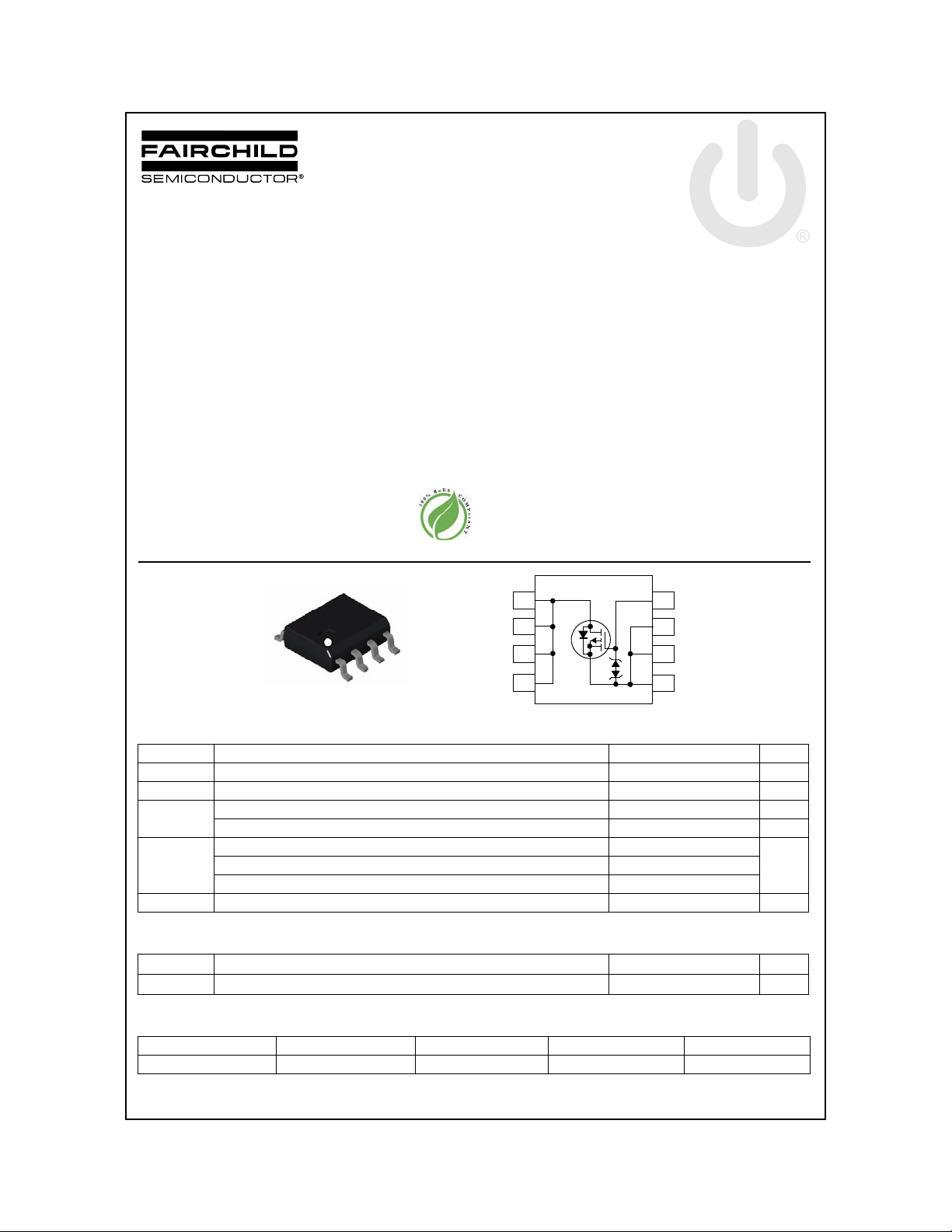
D
D
D
D
G
S
SO-8
MOSFET Maximum Ratings T
Symbol Parameter Ratings Units
V
DS
V
GS
I
D
P
D
, T
T
J
STG
Drain to Source Voltage -30 V
Gate to Source Voltage ±25 V
Drain Current -Continuous (Note1a) -14.5 A
-Pulsed -75 A
Power Dissipation for Single Operation (Note1a) 2.5
(Note1c) 1.0
Operating and Storage Temperature -55 to 150 °C
S
S
= 25°C unless otherwise noted
A
Features
Max r
Max r
Extended V
HBM ESD protection level of 6.5kV typical (note 3)
High performance trench technology for extremely low
r
DS(on)
High power and current handling capability
RoHS compliant
6
8
= 7.8m:VGS= -10V, ID = -14. 5A
DS(on)
= 12m:VGS= -4.5V, ID = -12A
DS(on)
range (-25V) for battery applications
GS
5
4
3
7
2
1
®
MOSFET
W (Note1b) 1.2
Thermal Characteristics
R
TJA
R
TJC
Thermal Resistance , Junction to Ambient (Note 1a) 50 °C/W
Thermal Resistance , Junction to Case (Note 1) 25 °C/W
Package Marking and Ordering Information
Device Marking Device Reel Size Tape Width Quantity
FDS6673BZ FDS6673BZ 13’’ 12mm 2500 units
©2009 Fairchild Semiconductor Corporation
FDS6673BZ Rev. B2
www.fairchildsemi.com1

Electrical Characteristics T
= 25°C unless otherwise noted
J
Symbol Parameter Test Conditions Min Typ Max Units
Off Characteristics
B
VDSS
'B
'T
I
DSS
I
GSS
VDSS
J
Drain to Source Breakdown Voltage ID = -250PA, VGS = 0V -30 V
Breakdown Voltage Temperature
Coefficient
ID = -250PA, referenced to
25°C
-20 mV/°C
Zero Gate Voltage Drain Current VDS = -24V, VGS= 0V -1 PA
Gate to Source Leakage Current VGS = ±25V, VDS= 0V ±10 PA
FDS6673BZ P-Channel PowerTrench
On Characteristics
V
GS(th)
'V
'T
r
DS(on)
g
FS
GS(th)
J
Gate to Source Threshold Voltage VGS = VDS, ID = -250PA -1 -1.9 -3 V
Gate to Source Threshold Voltage
Temperature Coefficient
Drain to Source On Resistance
Forward Transconductance VDS = -5V, ID = -14.5A 60 S
(Note 2)
Dynamic Characteristics
C
iss
C
oss
C
rss
Input Capacitance
Output Capacitance 600 800 pF
Reverse Transfer Capacitance 600 900 pF
Switching Characteristics
t
d(on)
t
r
t
d(off)
t
f
Q
Q
Q
Q
g
g
gs
gd
Turn-On Delay Time
Rise Time 16 29 ns
Turn-Off Delay Time 225 36 ns
Fall Time 105 167 ns
Total Gate Charge
Total Gate Charge
Gate to Source Gate Charge 8 nC
Gate to Drain Charge 23.5 nC
(Note 2)
ID = -250PA, referenced to
25°C
V
= -10V , ID = -14.5A 6.5 7.8
GS
= -4.5V, ID = -12A 9.6 12
V
GS
= -10V, ID = -14.5A
V
GS
= 125oC
T
J
= -15V, VGS = 0V,
V
DS
f = 1.0MHz
8.1 mV/°C
9.7 12
3500 4700 pF
14 26 ns
= -15V, ID = -1A
V
DD
V
= -10V, RGS = 6:
GS
V
= -15V, VGS = -10V,
DS
= -14.5A
I
D
= -15V, VGS = -5V,
V
DS
I
= -14.5A
D
88 124 nC
46 65 nC
m:
®
MOSFET
Drain-Source Diode Characteristics
V
SD
t
rr
Q
rr
Notes:
1: R
TJA
drain pins. R
Scale 1 : 1 on letter size paper
2: Pulse Test: Pulse Width < 300Ps, Duty Cycle < 2.0%.
3: The diode connected between the gate and source serves only as protection against ESD. No gate overvoltage rating is implied.
FDS6673BZ Rev. B2
Source to Drain Diode Forward Voltage VGS= 0V, IS= -2.1A -0.7 -1.2 V
Reverse Recovery Time IF = 14.5A, di/dt = 100A/Ps45ns
Reverse Recovery Charge IF = 14.5A, di/dt = 100A/Ps34nC
is the sum of the junction-to-case and case-to-ambient thermal resistance where the case thermal reference is defined as the solder mounting surface of the
is guaranteed by design while R
TJC
a) 50 oC/W (10 sec)
when mounted on a 1 in
pad of 2 oz copper
is determined by the user’s board design.
TCA
2
b) 105 oC/W when mounted
on a .04 in
copper
2
pad of 2 oz
o
C/W when mounted
c) 125
on a minimun pad
www.fairchildsemi.com2
 Loading...