Fairchild FDS5672 service manual

FDS5672
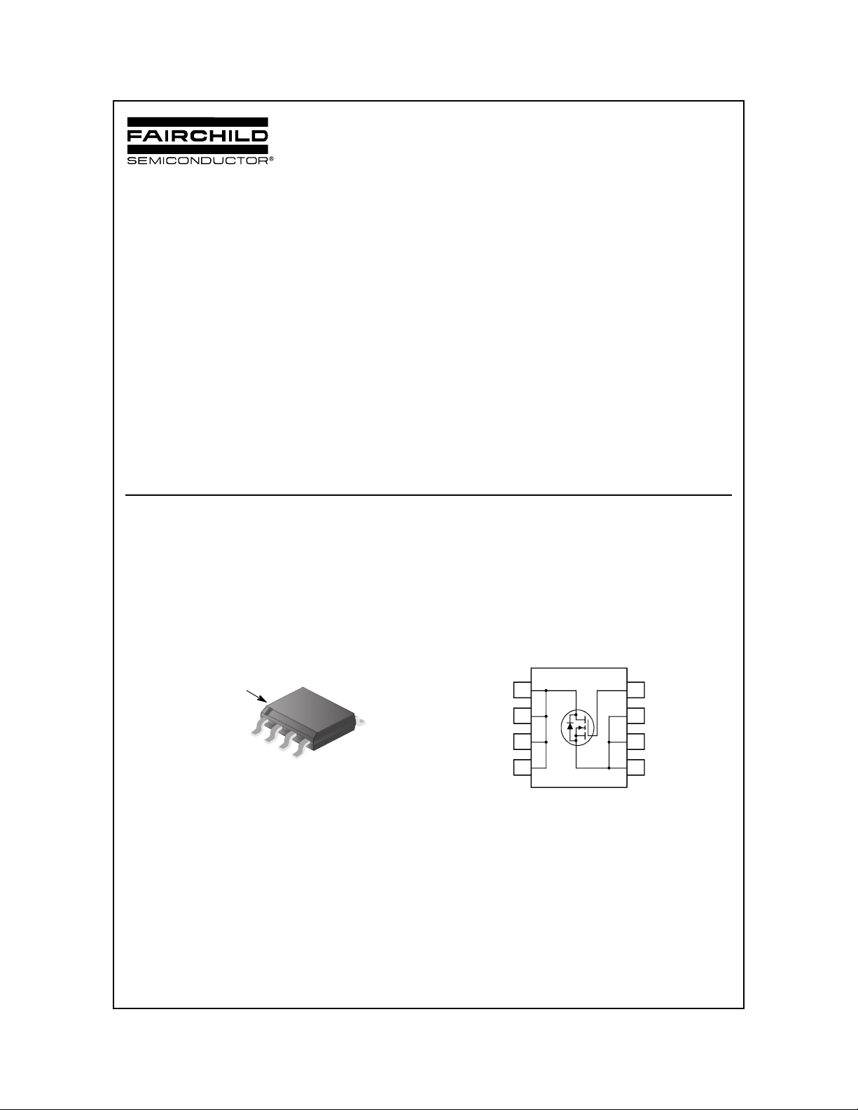
N-Channel PowerTrench® MOSFET
60V, 12A, 10mΩ
FDS5672 N-Channel PowerTrench
July 2005
Features
r
r
High performance trench technology for extremely low
r
Low gate charge
High power and current handling capability
DS(ON)
DS(ON)
DS(ON)
= 10mΩ, V
= 14mΩ, V
= 10V, ID = 12A
GS
= 6V, ID = 10A
GS
Applications
DC/DC converters
General Description
This N-Channel MOSFET has been designed specifically to
improve the overall efficiency of DC/DC converters using
either synchronous or conventional switching PWM
controllers. It has been optimized for low gate charge, low
r
and fast switching speed.
DS(ON)
®
MOSFET
Branding Dash
1
2
3
4
©2005 Fairchild Semiconductor Corporation
FDS5672 Rev. A
SO-8
5
5
6
7
8
1
4
3
2
1
www.fairchildsemi.com

FDS5672 N-Channel PowerTrench
MOSFET Maximum Ratings T
= 25°C unless otherwise noted
C
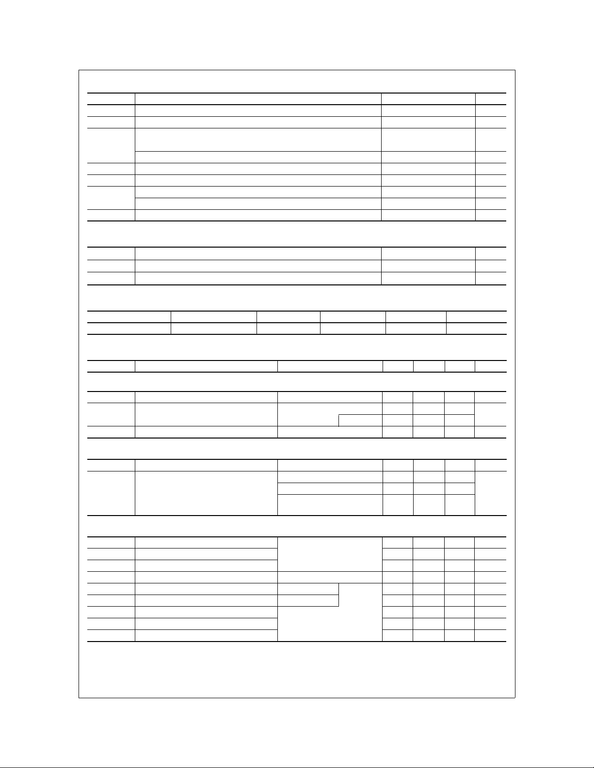
Symbol Parameter Ratings Units
V
DSS
V
GS
Drain to Source Voltage 60 V
Gate to Source Voltage ±20 V
Drain Current
I
D
Continuous (TC = 25 oC, VGS = 10V, R
Continuous (TC = 25 oC, VGS = 6V, R
= 50oC/W)
θJA
= 50oC/W) 10
θJA
12 A
Pulsed Figure 4 A
E
AS
P
D
TJ, T
STG
Single Pulse Avalanche Energy (Note 1) 245 mJ
Power dissipation 2.5 W
Derate above 25oC 20 mW/oC
Operating and Storage Temperature -55 to 150
Thermal Characteristics
R
θJC
R
θJA
R
θJA
Thermal Resistance Junction to Case (Note 2) 25
Thermal Resistance Junction to Ambient at 10 seconds (Note 3) 50
Thermal Resistance Junction to Ambient at 1000 seconds (Note 3) 85
Package Marking and Ordering Information
Device Marking Device Package Reel Size Tape Width Quantity
FDS5672 FDS5672 SO-8 330mm 12mm 2500 units
Electrical Characteristics T
Symbol Parameter Test Conditions Min Typ Max Units
= 25°C unless otherwise noted
C
o
C/W
o
C/W
o
C/W
o
C
®
MOSFET
Off Characteristics
B
I
DSS
I
GSS
VDSS
Drain to Source Breakdown Voltage ID = 250µA, VGS = 0V 60 - - V
Zero Gate Voltage Drain Current
Gate to Source Leakage Current VGS = ±20V - - ±100 nA
On Characteristics
V
GS(TH)
r
DS(ON)
Gate to Source Threshold Voltage VGS = VDS, ID = 250µA 2 - 4 V
Drain to Source On Resistance
Dynamic Characteristics
C
C
C
R
Q
Q
Q
Q
Q
ISS
OSS
RSS
G
g(TOT)
g(TH)
gs
gs2
gd
Input Capacitance
Output Capacitance - 410 - pF
Reverse Transfer Capacitance - 130 - pF
Gate Resistance VGS = 0.5V, f = 1MHz - 1.4 - Ω
Total Gate Charge at 10V VGS = 0V to 10V
Threshold Gate Charge VGS = 0V to 2V - 4.2 5.5 nC
Gate to Source Gate Charge - 9.4 - nC
Gate Charge Threshold to Plateau - 5.2 - nC
Gate to Drain “Miller” Charge - 9.3 - nC
VDS = 50V - - 1
VGS = 0V TC = 150oC - - 250
ID = 12A, V
= 10V - 0.0088 0.010
GS
ID = 10A, VGS = 6V, - 0.012 0.014
ID = 12A, V
T
= 150oC
C
VDS = 25V, VGS = 0V,
= 10V,
GS
- 0.016 0.023
- 2200 - pF
f = 1MHz
- 34 45 nC
VDD = 30V
ID = 12A
Ig = 1.0mA
µA
Ω
©2005 Fairchild Semiconductor Corporation
FDS5672 Rev. A
2
www.fairchildsemi.com

Resistive Switching Characteristic s (V
t
ON
t
d(ON)
t
r
t
d(OFF)
t
f
t
OFF
Turn-On Time
Turn-On Delay Time - 13 - ns
Rise Time - 20 - ns
Turn-Off Delay Time - 35 - ns
Fall Time - 14 - ns
Turn-Off Time - - 64 ns
= 10V)
GS
VDD = 30V, ID = 12A
VGS = 10V, RGS = 9.1Ω
- - 50 ns
Drain-Source Diode Characteristics
I
= 12A - - 1.25 V
V
SD
t
rr
Q
RR
Notes:
1: Starting TJ = 25°C, L = 1mH, IAS = 22A, VDD = 60V, VGS = 10V.
2: R
θJA
drain pins. R
3: R
θJA
Source to Drain Diode Voltage
Reverse Recovery Time ISD=12A, dISD/dt = 100A/µs - - 39 ns
Reverse Recovered Charge ISD=12A, dISD/dt = 100A/µs - - 40 nC
is the sum of the junction-to-cas e and cas e-to-am bient th ermal r esistance whe re the case therm al refer ence is defined a s the solder mounti ng surface of the
is measured with 1.0 in2 copper on FR-4 board.
is guaranteed by design while R
θJC
is determined by the user’s board design.
θJA
SD
ISD = 6A - - 1.0 V
FDS5672 N-Channel PowerTrench
®
MOSFET
©2005 Fairchild Semiconductor Corporation
FDS5672 Rev. A
3
www.fairchildsemi.com

FDS5672 N-Channel PowerTrench
Typical Characteristics T
1.2
1.0
0.8
0.6
0.4
0.2
POWER DISSIPATION MULTIPLIER
0
0255075100 150
TA, AMBIENT TEMPERATURE (oC)
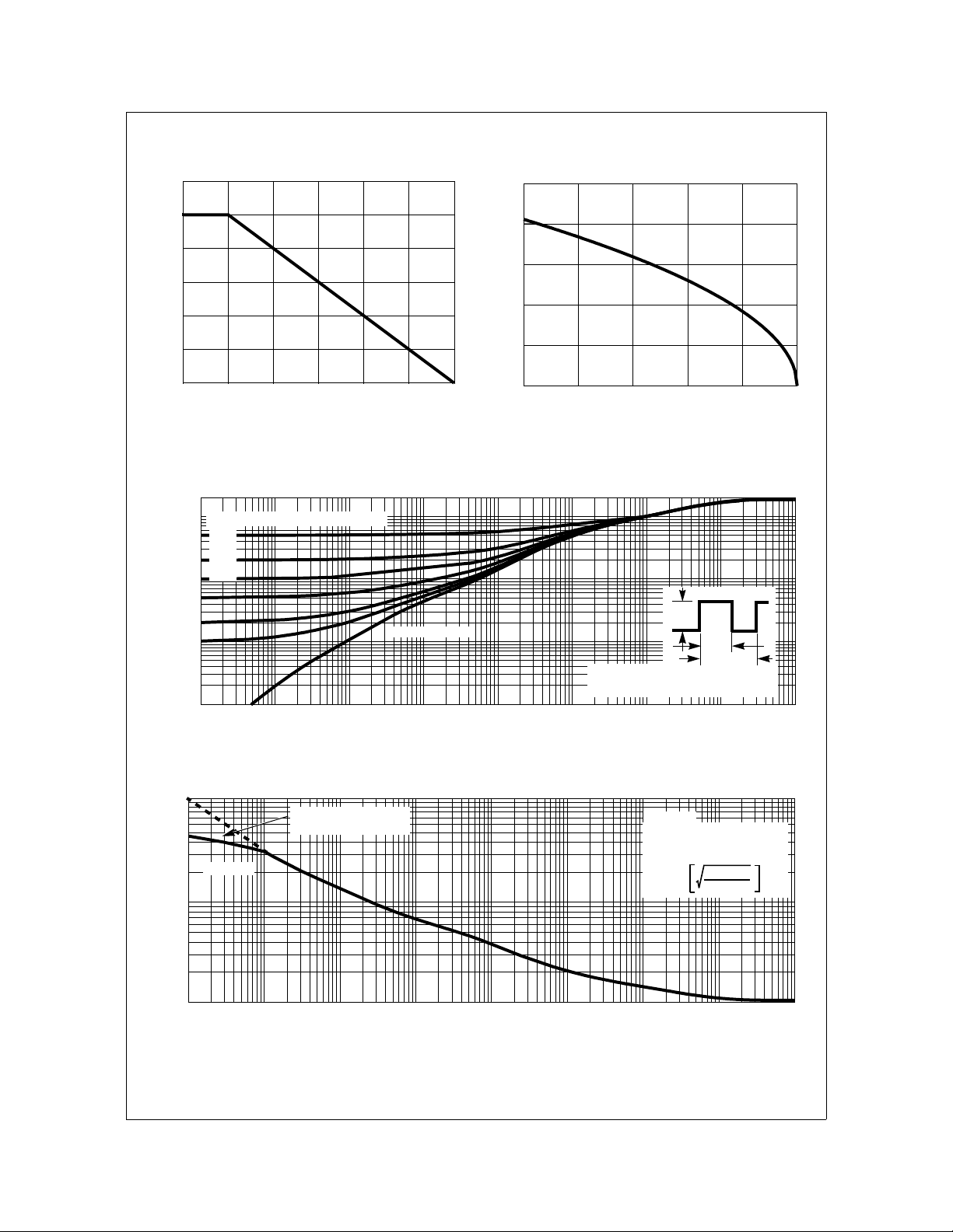
Figure 1.
Normalized Power Dissipation vs
= 25°C unless otherwise noted
C
125
Ambient Temperature
2
1
DUTY CYCLE - DESCENDING ORDER
0.5
0.2
0.1
0.05
0.02
0.01
0.1
15
12
9
6
, DRAIN CURRENT (A)
D
I
3
0
25 50 75 100 125 150
TA, AMBIENT TEMPERATURE (oC)
Figure 2.
Maximum Continuous Drain Current vs
V
= 10V
GS
Ambient Temperature
®
MOSFET
, NORMALIZED
θJA
Z
0.01
THERMAL IMPEDANCE
0.001
10
1100
100
, PEAK CURRENT (A)
DM
I
10
-5
10
-5
VGS = 10V
-4
10
Figure 3.
TRANSCONDUCTANCE
MAY LIMIT CURRENT
IN THIS REGION
-4
10
SINGLE PULSE
NOTES:
DUTY FACTOR: D = t
PEAK TJ = PDM x Z
-3
10
-2
10
t, RECTANGULAR PULSE DURATION (s)
-1
10
10
0
1
10
Normalized Maximum Transient Thermal Impedance
TA = 25oC
FOR TEMPERATURES
ABOVE 25
CURRENT AS FOLLOWS:
I = I
-3
10
Figure 4.
-2
10
t, PULSE WIDTH (s)
-1
10
Peak Current Capability
0
10
1
10
P
DM
1/t2
x R
θJA
θJA
o
C DERATE PEAK
25
t
1
t
+ T
2
10
150 - T
125
2
10
2
A
3
10
A
3
10
©2005 Fairchild Semiconductor Corporation
FDS5672 Rev. A
4
www.fairchildsemi.com
 Loading...