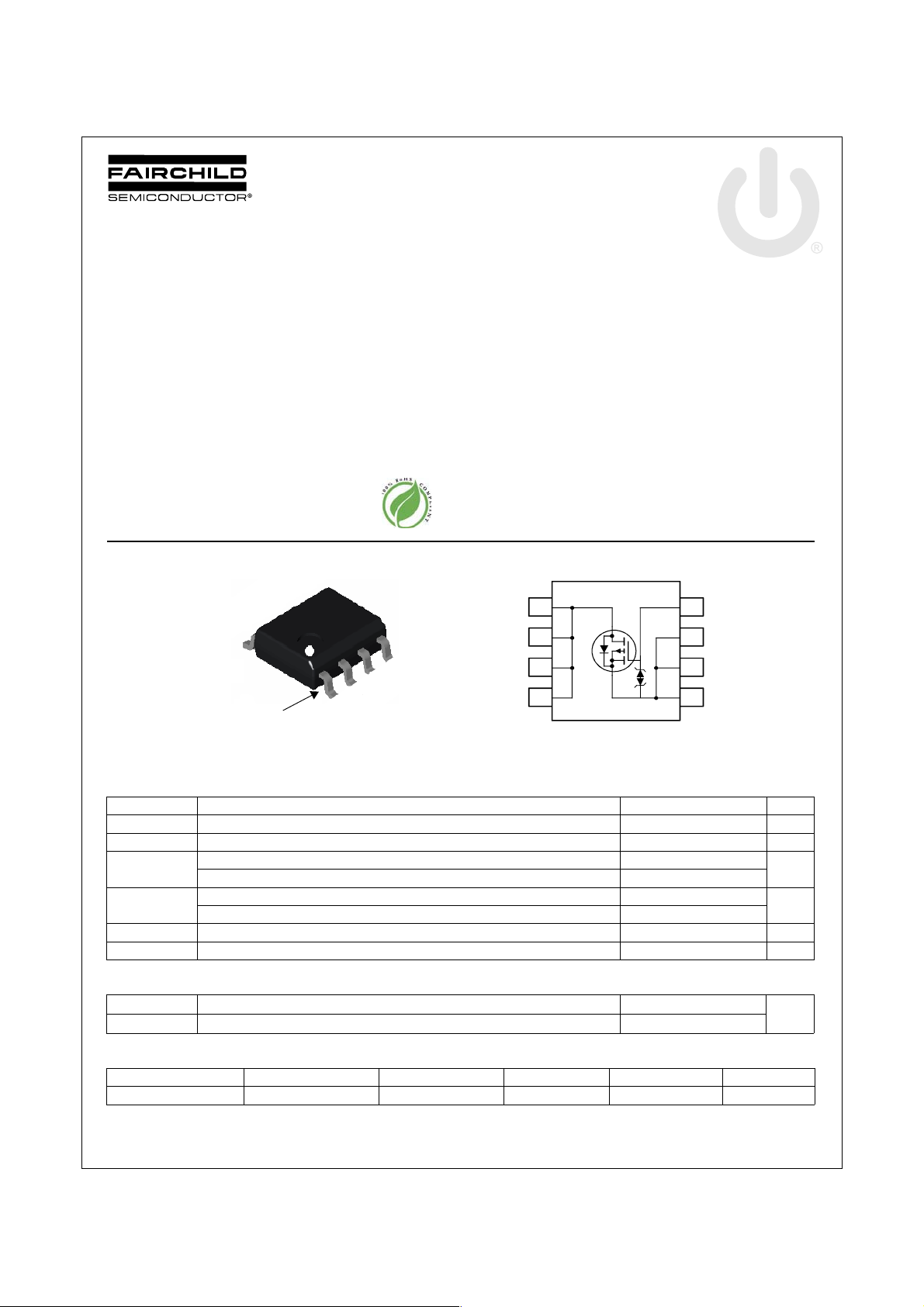
Fairchild FDS4435BZ, FDS4435BZ Schematics

FDS4435BZ
P-Channel PowerTrench® MOSFET
-30V, -8.8A, 20m:
Features
Max r
Max r
Extended V
HBM ESD protection level of ±3.8KV typical (note 3)
High performance trench technology for extremely low r
High power and current handling capability
Termination is Lead-free and RoHS compliant
= 20m: at VGS = -10V, ID = -8.8A
DS(on)
= 35m: at VGS = -4.5V, ID = -6.7A
DS(on)
range (-25V) for battery applications
GSS
D
D
D
DS(on)
D
April 2009
General Description
This P-Channel MOSFET is produced using Fairchild
®
Semiconductor’s advanced PowerTrench
been especially tailored to minimize the on-state resistance.
This device is well suited for Power Management and load
switching applications common in Notebook Computers and
Portable Battery Packs.
D
5
6
D
process that has
G
4
3
S
FDS4435BZ P-Channel PowerTrench
®
MOSFET
S
7
G
S
S
Pin 1
SO-8
MOSFET Maximum Ratings T
Symbol Parameter Ratings Units
V
DS
V
GS
I
D
P
D
E
AS
, T
T
J
STG
Drain to Source Voltage -30 V
Gate to Source Voltage ±25 V
Drain Current -Continuous TA= 25°C (Note 1a) -8.8
-Pulsed -50
Power Dissipation TA = 25°C (Note 1a) 2.5
Power Dissipation T
Single Pulse Avalanche Energy (Note 4) 24 mJ
Operating and Storage Junction Temperature Range -55 to +150 °C
S
= 25°C unless otherwise noted
A
D
8
D
= 25°C (Note 1b) 1.0
A
2
S
1
Thermal Characteristics
R
TJC
R
TJA
Thermal Resistance, Junction to Case 25
Thermal Resistance, Junction to Ambient (Note 1a) 50
Package Marking and Ordering Information
Device Marking Device Package Reel Size Tape Width Quantity
FDS4435BZ FDS4435BZ SO-8 13’’ 12mm 2500units
A
W
°C/W
©2009 Fairchild Semiconductor Corporation
FDS4435BZ Rev.C
1
1
www.fairchildsemi.com

FDS4435BZ P-Channel PowerTrench
Electrical Characteristics T
= 25°C unless otherwise noted
J
Symbol Parameter Test Conditions Min Typ Max Units
Off Characteristics
BV
'BV
'T
I
DSS
I
GSS
DSS
DSS
J
Drain to Source Breakdown Voltage ID = -250PA, VGS = 0V -30 V
Breakdown Voltage Temperature
Coefficient
I
= -250PA, referenced to 25°C -21 mV/°C
D
Zero Gate Voltage Drain Current VDS = -24V, VGS= 0V 1 PA
Gate to Source Leakage Current VGS = ±25V, VDS= 0V ±10 PA
On Characteristics
V
GS(th)
'V
'T
r
DS(on)
g
FS
GS(th)
J
Gate to Source Threshold Voltage VGS = VDS, ID = -250PA -1 -2.1 -3 V
Gate to Source Threshold Voltage
Temperature Coefficient
Static Drain to Source On Resistance
I
= -250PA, referenced to 25°C 6 mV/°C
D
V
= -10V, ID = -8.8A 16 20
GS
= -4.5V, ID = -6.7A 26 35
GS
= -10V, ID = -8.8A, TJ = 125°C 22 28
V
GS
Forward Transconductance VDS = -5V, ID = -8.8A 24 S
Dynamic Characteristics
C
iss
C
oss
C
rss
R
g
Input Capacitance
Output Capacitance 275 365 pF
Reverse Transfer Capacitance 230 345 pF
= -15V, VGS = 0V,
V
DS
f = 1MHz
Gate Resistance f = 1MHz 4.5 :
1385 1845 pF
Switching Characteristics
t
d(on)
t
r
t
d(off)
t
f
Q
Q
Q
Q
g
g
gs
gd
Turn-On Delay Time
Rise Time 612ns
Turn-Off Delay Time 30 48 ns
V
= -15V, ID = -8.8A,
DD
V
= -10V, R
GS
GEN
= 6:
10 20 ns
Fall Time 12 22 ns
Total Gate Charge VGS= 0V to -10V
Total Gate Charge VGS= 0V to -5V 16 23 nC
Gate to Source Charge 5.2 nC
VDD = -15V,
I
= -8.8A
D
28 40 nC
Gate to Drain “Miller” Charge 7.4 nC
m:V
®
MOSFET
Drain-Source Diode Characteristics
V
SD
t
rr
Q
rr
NOTES:
1. R
TJA
the user's board design.
2. Pulse Test: Pulse Width < 300Ps, Duty cycle < 2.0%.
3. The diode connected between the gate and source serves only as protection against ESD. No gate overvoltage rating is implied.
4. Starting T
©2009 Fairchild Semiconductor Corporation
FDS4435BZ Rev.C1
Source to Drain Diode Forward Voltage VGS= 0V, IS= -8.8A (Note 2) -0.9 -1.2 V
Reverse Recovery Time
Reverse Recovery Charge 23 35 nC
is determined with the device mou nted on a 1in2 pad 2 oz copper pad on a 1.5 x 1.5 in. board of FR-4 material. R
a. 50°C/W when mounted on
2
pad of 2 oz copper.
a 1 in
= 25°C, L = 1mH, IAS = -7A, VDD = -30V, VGS = -10V
J
= -8.8A, di/dt = 100A/Ps
I
F
2
29 44 ns
is guaranteed by design while R
TJC
b. 125°C/W when mounted on
a minimum pad of 2 oz copper.
is determined by
TCA
www.fairchildsemi.com

FDS4435BZ P-Channel PowerTrench
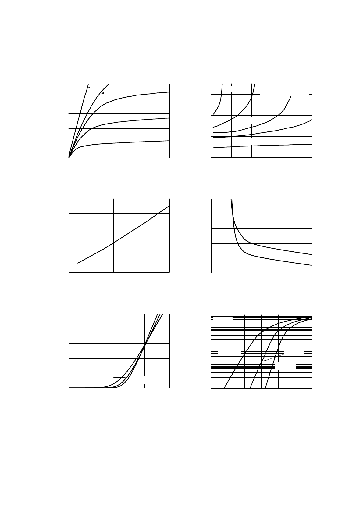
Typical Characteristics T
50
40
30
20
, DRAIN CURRENT (A)
D
-I
10
0
01234
-VDS, DRAIN TO SOURCE VOLTAGE (V)
Figure 1.
1.6
1.4
On-Region Characteristics Figure 2.
ID = -8.8A
V
= -10V
GS
1.2
1.0
NORMALIZED
0.8
DRAIN TO SOURCE ON-RESISTANCE
0.6
-75 -50 -25 0 25 50 75 100 125 150
TJ, JUNCTION TEMPERATURE (oC)
VGS = -10V
VGS = -5V
= 25°C unless otherwise noted
J
VGS = -4.5V
VGS = -4V
VGS = -3.5V
PULSE DURATION = 80Ps
DUTY CYCLE = 0.5%MAX
4.0
3.5
3.0
2.5
VGS = -3.5V
VGS = -4V
PULSE DURATION = 80Ps
DUTY CYCLE = 0.5%MAX
VGS = -4.5V
VGS = -5V
2.0
NORMALIZED
1.5
VGS = -10V
1.0
DRAIN TO SOURCE ON-RESISTANCE
0.5
0 1020304050
-ID, DRAIN CURRENT(A)
N o r m a l i z e d O n - R e s i s t a n c e
vs Drain Current and Gate Voltage
60
ID= -8.8A
50
(m:)
40
, DRAIN TO
30
DS(on)
r
20
SOURCE ON-RESISTANCE
10
246810
-VGS, GATE TO SOURCE VOLTAGE (V)
PULSE DURATION = 80Ps
DUTY CYCLE = 0.5%MAX
TJ= 125oC
TJ= 25oC
®
MOSFET
F i g u r e 3 . N o r m a l i z e d O n - R e s i s t a n c e
vs Junction Temperature
50
PULSE DURATION = 80Ps
DUTY CYCLE = 0.5%MAX
40
VDS= -5V
30
20
, DRAIN CURRENT (A)
D
10
-I
0
12345
TJ= 25oC
-VGS, GATE TO SOURCE VOLTAGE (V)
Figure 5. Transfer Characteristics
©2009 Fairchild Semiconductor Corporation
FDS4435BZ Rev.C
1
TJ= 150oC
TJ =-55oC
Figure 4.
O n - R es i s t a n c e vs G a t e t o
Source Voltage
100
VGS= 0V
10
1
0.1
TJ= 150oC
0.01
0.001
, REVERSE DRAIN CURRENT (A)
S
-I
0.0001
0.0 0.2 0.4 0.6 0.8 1.0 1.2
-VSD, BODY DIODE FORWARD VOLTAGE (V)
Figure 6.
S o u r ce t o D r a i n Di o d e
TJ = 25oC
TJ = -55oC
Forward Voltage vs Source Current
3
www.fairchildsemi.com
 Loading...