Fairchild FDS3692 service manual

FDS3692
N-Channel PowerTrench® MOSFET
100V, 4.5A, 60mΩ
FDS3692
September 2002
Features
•r
•Q
• Low Miller Charge
•Low Q
• Optimized eff iciency at high frequ encies
• UIS Capability (Single Pulse and Repetitive Pulse)
= 50mΩ (Typ.), V
DS(ON)
(tot) = 11nC (Typ.), V
g
Body Diode
RR
= 10V, ID = 4.5A
GS
= 10V
GS
Applications
• DC/DC converters and Off-Line UPS
• Distributed Power Architectures and VRMs
• PrimarySwitch for 24V and 48V Systems
• High Voltage Synchronous R ectifier
• Direct Injection / Diesel Injection Systems
• 42V Automotive Load Control
Formerly developmental type 82745
Branding Dash
1
2
3
4
5
• Electronic Valve Train Systems
5
6
7
8
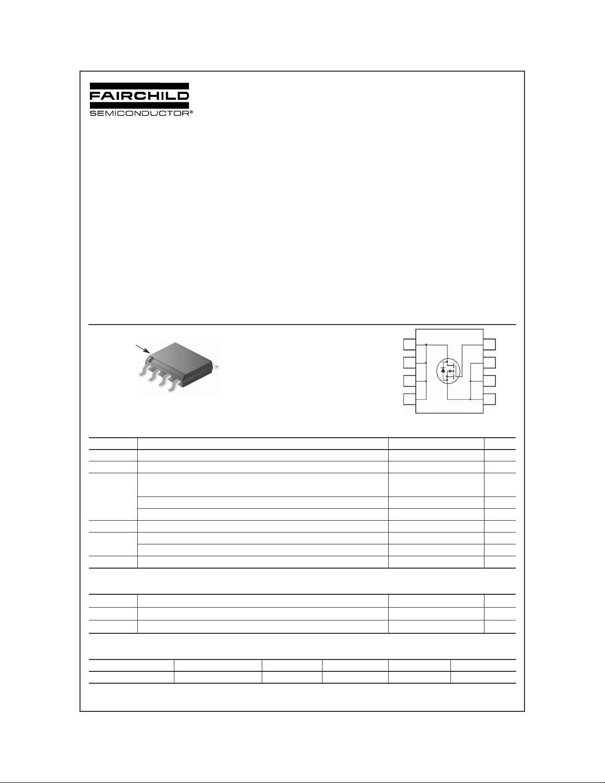
SO-8
MOSFET Maximum Ratings T
Symbol Parameter Ratings Units
V
DSS
V
GS
I
D
E
AS
P
D
T
, T
J
STG
Drain to Source Voltage 100 V
Gate to Source Voltage ±20 V
Drain Curr e nt
Continuous (T
Continuous (T
= 25oC, VGS = 10V, R
A
= 100oC, VGS = 10V, R
A
Pulsed Figure 4 A
Single Pulse Avalanche Energy (Note 1) 171 mJ
Power dissipation 2.5 W
o
Derate above 25
C20mW/
Operating and Storage Temperature -55 to 150
= 25°C unless otherwise noted
A
= 50oC/W)
θJA
= 50oC/W) 2.8 A
θJA
4.5 A
4
3
2
1
o
C
o
C
Thermal Characteristi cs
R
θJA
R
θJA
R
θJC
ThermalResistance,Junction to Ambientat 10 seconds (Note 3) 50
ThermalResistance,Junction to Ambientat 1000 seconds (Note 3) 85
ThermalResistance,Junctionto Case (Note 2) 25
Package Marking and Ordering Information
Device Marking Device Package Reel Size Tape Width Quantity
FDS369 2 FDS3692 SO-8 330mm 12mm 2500 un its
©2002 Fairchild Semiconductor Corporation
o
C/W
o
C/W
o
C/W
FDS3692 Rev. B

FDS3692
Electrical Characteristics T
= 25°C unl ess otherwise noted
A
Symbol Parameter Test Conditions Min Typ Max Units
Off Characteristics
B
I
DSS
I
GSS
VDSS
Drain t o Source Breakdown Volta ge ID = 250µA, VGS = 0V 100 - - V
V
= 80V - - 1
Zero Gate Voltage Drain Current
DS
= 0V TC = 150oC- - 250
V
GS
Gate to Source Leakage Current VGS = ±20V - - ±100 nA
On Characteristics
V
GS(TH)
r
DS(ON)
Gate to Source Threshold Voltage VGS = VDS, ID = 250µA2-4V
Drain to Source On Resistance
= 4.5A, V
I
D
I
= 2A, VGS = 6V - 0.064 0.096
D
I
= 4.5A, V
D
T
= 150oC
C
= 10V - 0.050 0.060
GS
= 10V,
GS
- 0.101 0.122
Dynamic Characteristics
C
C
C
Q
Q
Q
Q
Q
ISS
OSS
RSS
g(TOT)
g(TH)
gs
gs2
gd
Input Capacitance
Output Capacitance - 115 - pF
Reverse Transfer Capacitance - 27 - pF
= 25V, VGS = 0V,
V
DS
f = 1MHz
Total G ate Ch arg e at 10 V VGS = 0V to 10V
Threshold Gate Charge VGS = 0V to 2V - 1.4 1.9 nC
Gate to Source Gate Charge - 3.5 - nC
Gate Charge Threshold to Plateau - 2.1 - nC
V
DD
I
= 4.5A
D
I
= 1.0m A
g
= 50V
Gate to Drain “Miller” Charge - 2.8 - nC
-746- pF
-1115nC
µA
Ω
Switching Characteristics
t
ON
t
d(ON)
t
r
t
d(OFF)
t
f
t
OFF
Turn-On Time
Turn-On Delay Time - 9.8 - ns
Rise Time - 26 - ns
T u rn-Off Delay Time - 34 - ns
Fall Time - 26 - ns
Turn-Off Time - - 90 ns
(VGS = 10V)
V
= 50V, ID = 4.5A
DD
V
= 10V, RGS = 26Ω
GS
--54ns
Drain-Source Diode Characteristics
I
= 4.5A - - 1.25 V
V
SD
t
rr
Q
RR
Notes:
1: Starting T
2: R
θJA
drain pins. R
3: R
θJA
Source to Drain Di ode Voltage
Reverse Recovery Time ISD= 4.5A, dISD/dt= 100A/µs- - 47ns
Reverse Recovered Charge ISD= 4.5A, dISD/dt= 100A/µs- - 64nC
= 25°C, L = 38mH, IAS = 3A.
J
is the sum of the junction-to-case and cas e-to-a mbient thermal r esistance wher e the case thermal reference is defined as the solder mounting su rface of the
is measured with 1.0 in2 copper on FR-4 board
is guaranteed by design while R
θJC
is determined by the user’s board design.
θCA
SD
I
= 2A - - 1.0 V
SD
©2002 Fairchild Semiconductor Corporation FDS3692 Rev . B

FDS3692
Typical Characteristics T
= 25°C unl ess otherwise noted
A
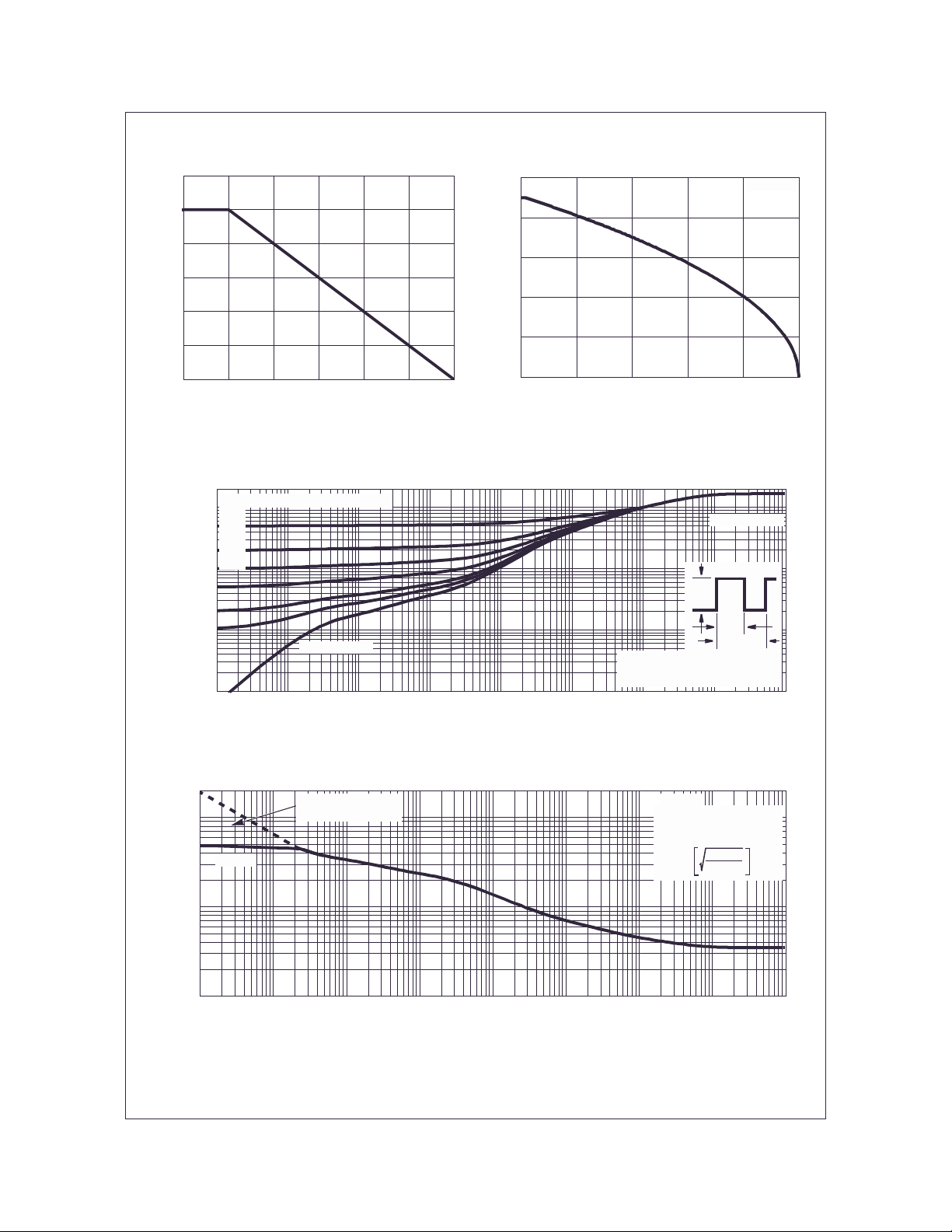
1.2
1.0
0.8
0.6
0.4
0.2
POWER DISSIPATION MULTIPLIER
0
0 25 50 75 100 150
TA, AMBIENT TEMPERATURE (oC)
Figure 1. Normalized Power Dissipation vs
Ambient Temperature
2
DUTY CYCLE - DESCENDING ORDER
1
0.5
0.2
0.1
0.05
0.02
0.01
0.1
, NORMALIZED
0.01
θJA
Z
THERMAL IMPEDANCE
0.001
-5
10
SINGLE PULSE
-4
10
-3
10
5
4
3
2
, DRAIN CURRENT (A)
D
I
1
0
125
25 50 75 100 125 150
Figure 2. Maximum Continuous Drain Curr ent vs
-2
10
t, RECTANGULAR PULSE DURATION (s)
-1
10
10
TC, CASE TEMPERATURE (oC)
Case Temperature
NOTES:
DUTY FACTOR: D = t
PEAK TJ = PDM x Z
0
1
10
V
= 10V
GS
R
=50oC/W
θJA
P
DM
t
1
t
2
1/t2
x R
+ T
θJA
θJA
A
2
10
3
10
Figure 3. Normalized Maximum Transient Thermal Impedance
200
100
TRANSCONDUCTANCE
MAY LIMIT CURRENT
IN THIS REGION
VGS = 10V
10
, PEAK CURRENT (A)
DM
I
1
-5
10
-4
10
-3
10
-2
10
t, PULSE WIDTH (s)
-1
10
0
10
TA = 25oC
FOR TEMPERATURES
o
ABOVE 25
CURRENT AS FOLLOWS:
I = I
25
1
10
10
C DERATE PEAK
150 - T
C
125
2
3
10
Figure 4. Peak Current Capability
©2002 Fairchild Semiconductor Corporation FDS3692 Rev . B

Typical Characteristics T
= 25°C unl ess otherwise noted
A
FDS3692
200
, DRAIN CURRENT (A)
I
D
0.01
100
10
1
0.1
SINGLE PULSE
TJ = MAX R ATED
T
OPERATION IN THIS
AREA MAY BE
LIMITED BY r
= 25oC
C
DS(ON)
110100
VDS, DRAIN TO SOURCE VOLTAGE (V)
10µs
100µs
1ms
10ms
100ms
1s
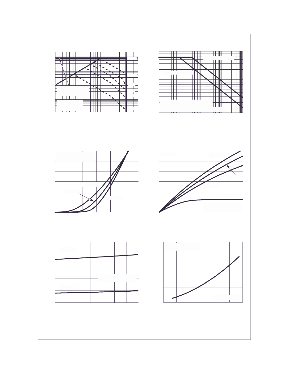
Figure 5. Forward Bias Safe Operating Area
30
PULSE DURATION = 80µs
DUTY CYCLE = 0.5% MAX
V
= 15V
DD
25
20
15
10
, DRAIN CURRENT (A)
D
I
5
0
TJ = 25oC
3.5 4.0 4.5 5.0 5.5 6.0 6.5
TJ = 150oC
TJ = -55oC
VGS, GATE TO SOURCE VOLTAGE (V)
7
STARTING TJ = 25oC
STARTING TJ = 150oC
1
, AVALANCHE CURRENT (A)
If R = 0
AS
I
tAV = (L)(IAS)/(1.3*RATED BV
If R ≠ 0
t
= (L/R)ln[(IAS*R)/(1.3*RATED BV
AV
3000.1
0.1
0.01 0.1 1 10 100
tAV, TIME IN AVALANCHE (ms)
DSS
- VDD)
- VDD) +1]
DSS
NOTE: Refer to Fairchild Application Notes AN7514 and AN7515
Figure 6. Unclamped Inductive Switching
Capability
30
TA = 25oC
25
20
15
10
, DRAIN CURRENT (A)
D
I
5
0
0 0.5 1.0 1.5 2.0
VDS, DRAIN TO SOURCE VOLTAGE (V)
VGS = 10V
VGS = 6V
PULSE DURATION = 80µs
DUTY CYCLE = 0.5% MAX
VGS = 7V
VGS = 5V
Figure 7. Transfer Characteristics Figure 8. Saturation Characteristics
70
VGS = 6V
65
60
55
VGS = 10V
50
45
DRAIN TO SOURCE ON RESISTANCE (m Ω)
1.01.52.02.53.03.54.04.5
I
, DRAIN CURRENT (A)
D
PULSE DURATION = 80µs
DUTY CYCLE = 0.5% MAX
Figure 9. Drain to So urce On Resistanc e v s Drai n
Current
©2002 Fairchild Semiconductor Corporation FDS3692 Rev . B
2.5
PULSE DURATION = 80µs
DUTY CYCLE = 0.5% MAX
2.0
1.5
ON RESISTANCE
1.0
NORMALIZED DRAIN TO SOURCE
0.5
-80 -40 0 40 80 120 160
TJ, JUNCTION TEMPERATURE (oC)
VGS = 10V, ID = 4.5A
Figure 10. Normalized Drain to Source On
Resistance vs Junction Temperature
 Loading...