Fairchild FDS2670 service manual

FDS2670
200V N-Channel PowerTrench
MOSFET
FDS2670
August 2001
General Description
This N-Channel MOSFET has been designed
specifically to improve the overall efficiency of DC/ DC
converters using either synchronous or conventional
switching PWM controller s .
These MOSFETs feature faster switching and lower
gate charge than other MOSFETs with comparable
specifications.
RDS
(ON)
The result is a MOSFET that is easy and safer to drive
(even at very high frequencies), and DC/DC power
supply designs with higher overall efficiency.
D
D
Features
• 3.0 A, 200 V. R
• Low gate charge
• Fast switching speed
• High performance trench technology for extremely
low R
DS(ON)
• High power and current handling capability
5
= 130 mΩ @ VGS = 10 V
DS(ON)
4
D
D
G
S
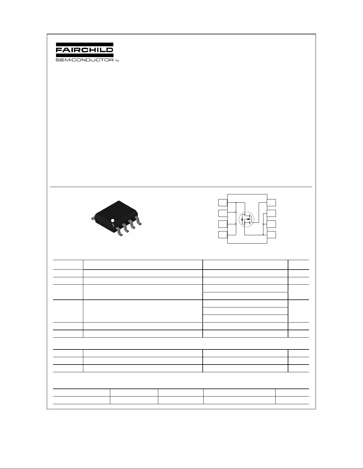
SO-8
S
S
Absolute Maximum Ratings T
=25oC unless otherwise noted
A
6
7
8
3
2
1
Symbol Parameter Ratings Units
V
DSS
V
GSS
I
D
P
D
dv/dt Peak Diode Recovery dv/dt (Note 3) 3.2 V/ns
TJ, T
STG
Drain-Source Voltage 200 V
Gate-Source Voltage
Drain Current – Continuous (Note 1a) 3.0 A
– Pulsed 20
Power Dissipation for Single Operation (Note 1a) 2.5
(Note 1b)
(Note 1c)
Operating and Storage Junction Temperature Range
±20
1.2
1.0
−55 to +150 °C
V
W
Thermal Characteristics
R
θJA
R
θJA
R
θJC
Thermal Resistance, Junction-to-Ambient (Note 1a) 50
Thermal Resistance, Junction-to-Ambient (Note 1c) 125
Thermal Resistance, Junction-to-Case (Note 1) 25
Package Marking and Ordering Information
Device Marking Device Reel Size Tape width Quantity
FDS2670 FDS2670 13’’ 12mm 2500 units
2001 Fairchild Semiconductor Corporation
°C/W
°C/W
°C/W
FDS2670 Rev C1(W)

FDS2670
Electrical Characteristics T
= 25°C unless otherwise noted
A
Symbol Parameter Test Conditions Min Typ Max Units
Drain-Source Avalanche Ratings (Note 1)
W
DSS
I
AR
Single Pulse Drain-Source
Avalanche Energy
Maximum Drain-Source Avalanche
Current
VDD = 100 V, ID = 3.0 A 375 mJ
3.0 A
Off Characteristics
BV
DSS
∆BVDSS
∆T
J
I
DSS
I
GSSF
I
GSSR
Drain–Source Breakdown Voltage
Breakdown Voltage Temperature
Coefficient
= 0 V, ID = 250 µA
V
GS
= 250 µA, Referenced to 25°C
I
D
Zero Gate Voltage Drain Current VDS = 160 V, VGS = 0 V 1
Gate–Body Leakage, Forward VGS = 20 V, VDS = 0 V 100 nA
Gate–Body Leakage, Reverse VGS = –20 V VDS = 0 V –100 nA
200 V
214
mV/°C
µA
On Characteristics (Note 2)
V
GS(th)
∆VGS(th)
∆T
R
DS(on)
I
D(on)
g
FS
Gate Threshold Voltage
Gate Threshold Voltage
Temperature Coefficient
J
Static Drain–Source
On–Resistance
V
= VGS, ID = 250 µA
DS
= 250 µA, Referenced to 25°C
I
D
VGS = 10 V, ID = 3.0 A
=10 V, ID =3.0 A, TJ =125°C
V
GS
244.5V
–10
100
205
On–State Drain Current VGS = 10 V, VDS = 10 V 20 A
Forward Transconductance VDS = 10 V, ID = 3.0 A 15 S
130
275
mV/°C
mΩ
Dynamic Characteri stics
C
iss
C
oss
C
rss
Input Capacitance 1228 pF
Output Capacitance 112 pF
Reverse Transfer Capacitance
V
= 100 V, V
DS
f = 1.0 MHz
GS
= 0 V,
17 pF
Switching Characteristics (Note 2)
t
t
t
t
Q
Q
Q
d(on)
r
d(off)
f
g
gs
gd
Turn–On Delay Time 13 23 ns
Turn–On Rise Time 8 16 ns
V
= 100 V, ID = 1 A,
DD
= 10 V, R
V
GS
GEN
= 6 Ω
Turn–Off Delay Time 30 48 ns
Turn–Off Fall Time
Total Gate Charge 27 43 nC
Gate–Source Charge 7 nC
V
= 100 V, ID = 3 A,
DS
= 10 V
V
GS
Gate–Drain Charge
Drain–Source Diode Characteristics and Maximum Ratings
I
S
V
SD
Maximum Continuous Drain–Source Diode Forward Current 2.1 A
Drain–Source Diode Forward
Voltage
= 0 V, IS = 2.1 A (Note 2) 0.7 1.2 V
V
GS
25 40 ns
10 nC
FDS2670 Rev C1(W)
 Loading...