

tm
FDPF3860T
N-Channel PowerTrench® MOSFET
100V, 20A, 38.2mΩ
FDPF3860T N-Channel PowerTrench
March 2008
Description
•R
• Fast switching speed
• Low gate charge
• High performance trench technology for extremely low R
• High power and current handling capability
• RoHS compliant
MOSFET Maximum Ratings T
V
DSS
V
GSS
I
D
I
DM
E
AS
I
AR
E
AR
dv/dt Peak Diode Recovery dv/dt (Note 3) 15 V/ns
P
D
, T
T
J
T
L
= 38.2mΩ ( MAX ) @ VGS = 10V, ID = 5.9A
DS(on)
DS(on)
D
G
S
Symbol Parameter Ratings Units
Drain to Source Voltage 100 V
Gate to Source Voltage ±20 V
Drain Current
Drain Current - Pulsed (Note 1) 80 A
Single Pulsed Avalanche Energy (Note 2) 278 mJ
Avalanche Current (Note 1) 20 A
Repetitive Avalanche Energy (Note 1) 3.4 mJ
Power Dissipation
STG
Operating and Storage Temperature Range -55 to +150
Maximum Lead Temperature for Soldering Purpose,
1/8” from Case for 5 Seconds
TO-220F
o
= 25
C
- Continuous (T
- Continuous (T
(T
C
- Derate above 25
C unless otherwise noted
= 25oC) 33.8 W
General Description
This N-Channel MOSFET is produced using Fairchild Semiconductor’s advanced PowerTrench process that has been especially tailored to minimize the on-state resistance and yet
maintain superior switching performance.
Application
• DC to AC converters / Synchronous Rectification
D
G
S
= 25oC) 20
C
= 100oC) 12.7
C
o
C0.27W/
300
o
o
®
MOSFET
A
o
C
C
C
Thermal Characteristics
Symbol Parameter Ratings Units
R
θJC
R
θJA
©2008 Fairchild Semiconductor Corporation
FDPF3860T Rev. A
Thermal Resistance, Junction to Case 3.7
Thermal Resistance, Junction to Ambient 62.5
o
C/W
www.fairchildsemi.com1
Package Marking and Ordering Information
Device Marking Device Package Reel Size Tape Width Quantity
FDPF3860T FDPF3860T TO-220F - - 50
FDPF3860T N-Channel PowerTrench
Electrical Characteristics T
= 25oC unless otherwise noted
C
Symbol Parameter Test Conditions Min. Typ. Max. Units
Off Characteristics
BV
∆BV
∆T
I
DSS
I
GSS
DSS
DSS
J
Drain to Source Breakdown Voltage ID = 250µA, VGS = 0V, TJ = 25oC 100 - - V
Breakdown Voltage Temperature
Coefficient
Zero Gate Voltage Drain Current
Gate to Body Leakage Current VGS = ±20V, V
I
= 250µA, Referenced to 25oC-0.1-V/
D
V
= 80V, V
DS
= 48V, TC = 150oC - - 500
V
DS
= 0V - - 1
GS
= 0V - - ±100 nA
DS
On Characteristics
V
GS(th)
R
DS(on)
g
FS
Gate Threshold Voltage VGS = VDS, ID = 250µA2.5-4.5V
Static Drain to Source On Resistance VGS = 10V, ID = 5.9A - 29.1 38.2 mΩ
Forward Transconductance VDS = 10V , ID = 5.9A (Note 4) -21-S
Dynamic Characteristics
C
iss
C
oss
C
rss
Input Capacitance
Output Capacitance - 145 190 pF
Reverse Transfer Capacitance - 60 90 pF
Switching Characteristics
t
d(on)
t
r
t
d(off)
t
f
Q
Q
Q
g(tot)
gs
gd
Turn-On Delay Time
Turn-On Rise Time - 17 45 ns
Turn-Off Delay Time - 24 60 ns
Turn-Off Fall Time - 7 25 ns
Total Gate Charge at 10V
Gate to Source Gate Charge - 7 - nC
Gate to Drain “Miller” Charge - 8 - nC
= 25V, VGS = 0V
V
DS
f = 1MHz
= 50V, ID = 5.9A
V
DD
V
= 10V, R
GS
(Note 4, 5)
V
= 80V, ID = 5.9A
DS
V
= 10V
GS
(Note 4, 5)
GEN
= 6Ω
- 1350 1800 pF
-1540ns
-2335nC
µA
o
C
®
MOSFET
Drain-Source Diode Characteristics
I
S
I
SM
V
SD
t
rr
Q
rr
Notes:
1. Repetitive Rating: Pulse width limited by maximum junction temperature
2. L =16mH, IAS = 5.9A, VDD = 50V, RG = 25Ω, Starting TJ = 25°C
3. ISD ≤ 5.9A, di/dt ≤ 200A/µs, VDD ≤ BV
4. Pulse Test: Pulse width ≤ 300µs, Duty Cycle ≤ 2%
5. Essentially Independent of Operating Temperature Typical Characteristics
FDPF3860T Rev. A
Maximum Continuous Drain to Source Diode Forward Current - - 20 A
Maximum Pulsed Drain to Source Diode Forward Current - - 80 A
Drain to Source Diode Forward Voltage V
Reverse Recovery Time
Reverse Recovery Charge - 56 - nC
, Starting TJ = 25°C
DSS
= 0V, I
GS
V
= 0V, I
GS
dI
/dt = 100A/µs (Note 4)
F
= 5.9A - - 1.3 V
SD
= 5.9A
SD
2
-40-ns
www.fairchildsemi.com
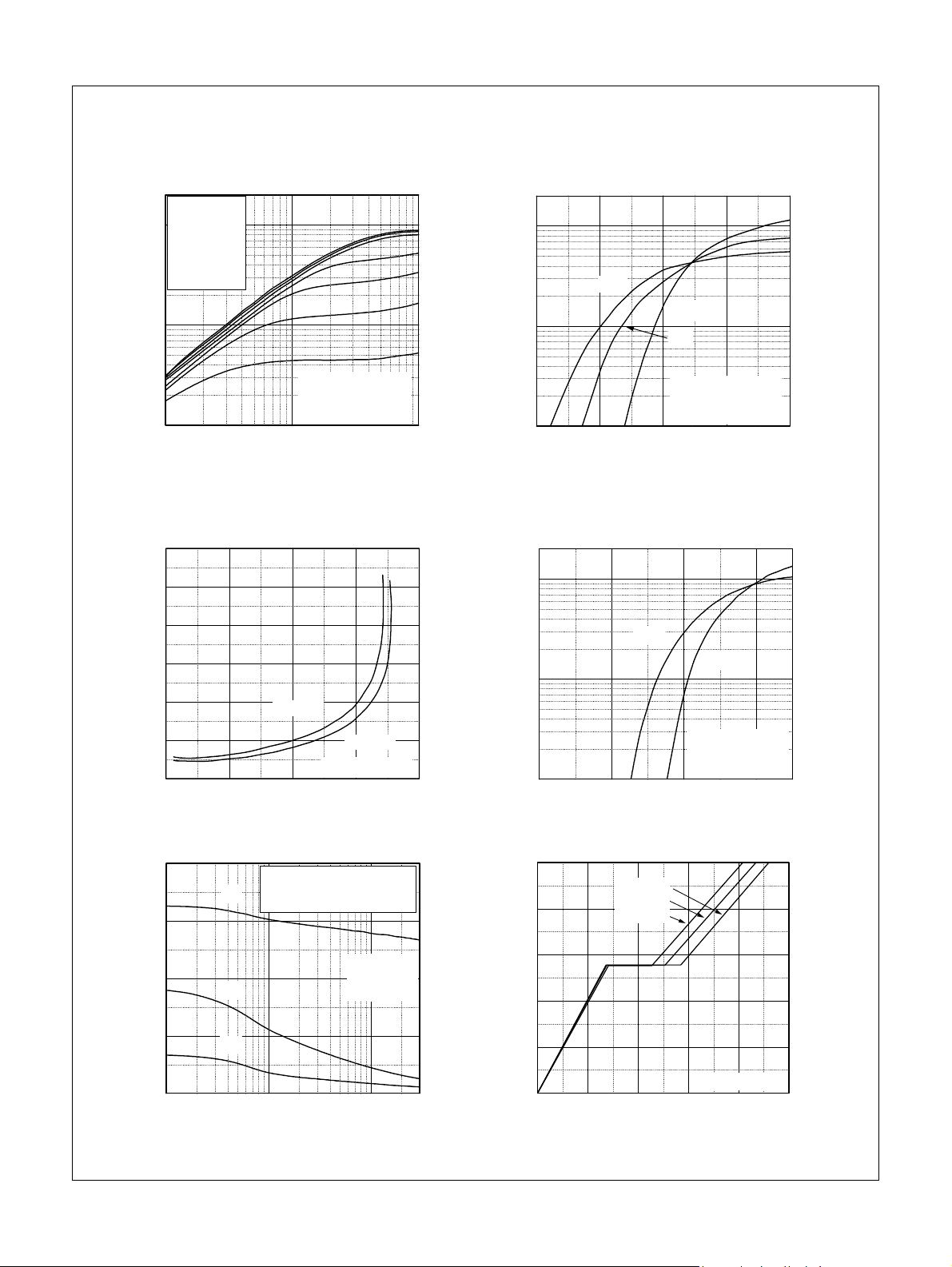
Typical Performance Characteristics
Figure 1. On-Region Characteristics Figure 2. Transfer Characteristics
200
V
= 15.0 V
GS
10.0 V
100
8.0 V
7.0 V
6.5 V
6.0 V
5.5 V
10
,Drain Current[A]
D
I
*Notes:
1. 250
µs Pulse Test
= 25oC
2. T
1
0.1 1 10
C
VDS,Drain-Source Voltage[V]
Figure 3. On-Resistance Variation vs. Figure 4. Body Diode Forward Voltage
Drain Current and Gate Voltage Variation vs. Source Current
and Temperature
0.14
0.12
200
100
150oC
-55oC
10
,Drain Current[A]
D
I
1
45678
25oC
*Notes:
1. V
= 20V
DS
2. 250µs Pulse Test
VGS,Gate-Source Voltage[V]
200
100
FDPF3860T N-Channel PowerTrench
®
MOSFET
0.10
[Ω],
0.08
DS(ON)
R
0.06
0.04
Drain-Source On-Resistance
0.02
0 25 50 75 100
VGS = 10V
*Note: TJ = 25oC
ID, Drain Current [A]
VGS = 20V
10
, Reverse Drain Current [A]
S
I
1
0.00.40.81.2
VSD, Body D io de Forward Vo lta g e [V]
150oC
25oC
*Notes:
1. VGS = 0V
2. 250
µs Pulse Test
Figure 5. Capacitance Characteristics Figure 6. Gate Charge Characteristics
2000
C
= Cgs + Cgd (Cds = shorted)
iss
C
= Cds + C
C
oss
iss
C
= C
rss
gd
1500
1000
Capacitances [pF]
500
0
0.1 1 10
C
oss
C
rss
VDS, Drain-Source Voltage [V ]
gd
*Note:
1. V
2. f = 1MHz
= 0V
GS
30
10
VDS = 80V
V
= 50V
DS
V
8
DS
= 25V
6
4
, Gate-Source Voltage [V]
GS
V
2
*Note: ID = 5.9A
0
0 5 10 15 20 25
Qg, Total Gate Charge [nC]
1.4
FDPF3860T Rev. A
3
www.fairchildsemi.com
 Loading...