Fairchild FDP8447L service manual

tm
FDP8447L
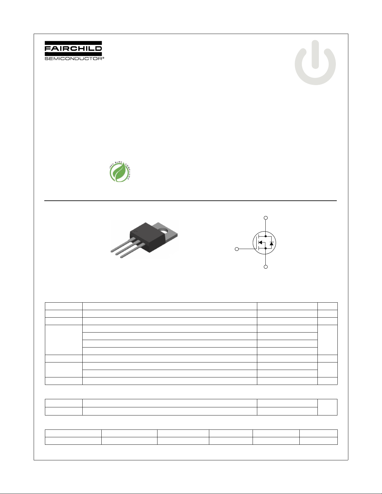
N-Channel PowerTrench® MOSFET
40V, 50A, 8.7mΩ
Features
Max r
Max r
Fast Switching
RoHS Compliant
= 8.7mΩ at VGS = 10V, ID = 14A
DS(on)
= 11.2mΩ at VGS = 4.5V, ID = 11A
DS(on)
General Description
This N-Channel MOSFET has been produced using Fairchild
Semiconductor’s proprietary PowerTrench technology to deliver
low
r
and optimized BV
DS(on)
performance benefit in the application.
Applications
Inverter
Power Supplies
May 2007
capability to offer superior
DSS
D
FDP8447L N-Channel PowerTrench
®
MOSFET
G
D
S
MOSFET Maximum Ratings T
Symbol Parameter Ratings Units
V
DS
V
GS
I
D
E
AS
P
D
, T
T
J
STG
Drain to Source Voltage 40 V
Gate to Source Voltage ±20 V
Drain Current -Continuous (Package limited) TC = 25°C 50
-Continuous (Silicon limited) T
-Continuous T
-Pulsed 100
Drain-Source Avalanche Energy (Note 3) 153 mJ
Power Dissipation TC = 25°C 60
Power Dissipation T
Operating and Storage Junction Temperature Range -55 to +150 °C
= 25°C unless otherwise noted
C
TO-220
FDP Series
= 25°C 65
C
= 25°C (Note 1) 12
A
= 25°C (Note 1) 2
A
G
S
Thermal Characteristics
R
θJC
R
θJA
Thermal Resistance, Junction to Case 2.1
Thermal Resistance, Junction to Ambient (Note 1) 62.5
Package Marking and Ordering Information
A
W
°C/W
Device Marking Device Package Reel Size Tape Width Quantity
FDP8447L FDP8447L TO-220AB Tube N/A 50units
©2007 Fairchild Semiconductor Corporation
FDP8447L Rev.B
1
www.fairchildsemi.com

FDP8447L N-Channel PowerTrench
Electrical Characteristics T
= 25°C unless otherwise noted
J
Symbol Parameter Test Conditions Min Typ Max Units
Off Characteristics
BV
DSS
∆BV
DSS
∆T
J
I
DSS
I
GSS
On Characteristics
V
GS(th)
∆V
GS(th)
∆T
J
r
DS(on)
g
FS
Drain to Source Breakdown Voltage ID = 250µA, VGS = 0V 40 V
Breakdown Voltage Temperature
Coefficient
ID = 250µA, referenced to 25°C 34 mV/°C
Zero Gate Voltage Drain Current VDS = 32V, 1 µA
Gate to Source Leakage Current VGS = ±20V, V
= 0V ±100 nA
DS
Gate to Source Threshold Voltage VGS = VDS, ID = 250µA 1 1.7 3 V
Gate to Source Threshold Voltage
Temperature Coefficient
Static Drain to Source On Resistance
Forward Transconductance VDD = 5V, ID = 14A 74 S
ID = 250µA, referenced to 25°C -6 mV/°C
VGS = 10V, ID = 14A 7.7 8.7
VGS = 10V, ID = 14A, TJ = 125°C 12.1 13.7
Dynamic Characteristics
C
iss
C
oss
C
rss
R
g
Input Capacitance
Output Capacitance 245 325 pF
Reverse Transfer Capacitance 150 225 pF
VDS = 20V, VGS = 0V,
f = 1MHz
1880 2500 pF
Gate Resistance f = 1MHz 1.4 Ω
Switching Characteristics
t
d(on)
t
r
t
d(off)
t
f
Q
Q
Q
Q
g
g
gs
gd
Turn-On Delay Time
Rise Time 7 14 ns
Turn-Off Delay Time 28 45 ns
VDD = 20V, ID = 14A,
VGS = 10V, R
GEN
= 6Ω
9 18 ns
Fall Time 4 10 ns
Total Gate Charge V
Total Gate Charge V
Gate to Source Charge 4.7 nC
= 0V to 10V
GS
= 0V to 5V 19 27 nC
GS
VDD = 20V,
ID = 14A
35 49 nC
Gate to Drain “Miller” Charge 6.2 nC
mΩVGS = 4.5V, ID = 11A 8.9 11.2
®
MOSFET
Drain-Source Diode Characteristics
V
SD
t
rr
Q
rr
NOTES:
1. R
is the sum of the junction-to-case and case -to- ambient thermal resistance where the case thermal reference is defined as the s olde r m ount i ng sur f ace o f the dr a in pi n s .
θJA
is guaranteed by design while R
R
θJC
2. Pulse Test: Pulse Width < 300µs, Duty cycle < 2.0%.
3. Starting T
©2007 Fairchild Semiconductor Corporation
FDP8447L Rev.B
Source to Drain Diode Forward Voltage V
Reverse Recovery Time
Reverse Recovery Charge 22 33 nC
is determined by the user’s board design.
θJA
= 25°C, L = 1mH, IAS = 17.5A, VDD = 40V, V
J
GS
= 10V.
= 0V, IS = 14A (Note 2) 0.8 1.2 V
GS
IF = 14A, di/dt = 100A/µs
2
28 42 ns
www.fairchildsemi.com
 Loading...