Fairchild FDP8440 service manual

tm
FDP8440
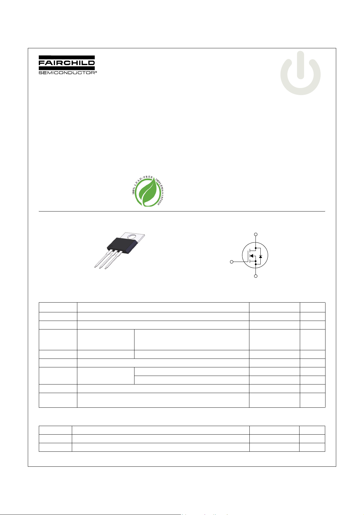
N-Channel PowerTrench
40V, 277A, 2.2mΩ
®
MOSFET
FDP8440 N-Channel PowerTrench
January 2009
Features
•R
•Q
• Low Miller Charge
•Low Q
• UIS Capability (Single Pulse and Repetitive Pulse)
•RoHS Compliant
MOSFET Maximum Ratings
= 1.64mΩ (Typ.)@ VGS = 10V, ID = 80A
DS(on)
= 345nC (Typ.)@ VGS = 10V
g(tot)
Body Diode
RR
G D S
TO-220
FDP Series
TC = 25oC unless otherwise noted
Application
• Automotive Engine Control
• Powertrain Management
• Motors, Solenoids
• Electronic Steering
• Integrated Starter/ Alternator
• Distributed Power Architectures and VRMs
• Primary Switch for 12V Systems
D
G
S
®
MOSFET
Symbol Parameter Ratings Units
V
DSS
V
GSS
I
D
I
DM
E
AS
P
D
T
J, TSTG
T
L
*Calculated continuous current based on maximum allowable junction temperature. Package limitation current is 100A.
Drain to Source Voltage 40 V
Gate to Source Voltage ±20 V
D r a i n C u rr e n t
Drain Current - Pulsed (Note 1) 500 A
Single Pulsed Avalanche Energy (Note 2) 1682 mJ
Power Dissipation
Operating and Storage Temperature Range -55 to +175
Maximum Lead Temperature for Soldering Purpose,
1/8” from Case for 5 Seconds
- Continuous (T
- Continuous (T
- Continuous (T
(T
= 25oC) 306 W
C
- Derate above 25
= 25oC, Silicon Limited)
C
= 100oC, Silicon Limited)
C
= 25oC, Package Limited)
C
o
C2.04W/
277*
196*
100
300
A
o
o
o
C
C
C
Thermal Characteristics
R
θJC
R
θCS
R
θJA
©2009 Fairchild Semiconductor Corporation 1 www.fairchildsemi.com
FDP8440 Rev. A6
Thermal Resistance, Junction to Case 0.49
Thermal Resistance, Case to Sink (Typ.) 0.5
Thermal Resistance, Junction to Ambient 62.5
o
C/W
o
C/W
o
C/W

Package Marking and Ordering Information
Device Marking Device Package Reel Size Tape Width Quantity
FDP8440 FDP8440 TO-220 N/A N/A 50units
FDP8440 N-Channel PowerTrench
Electrical Characteristics T
= 25°C unless otherwise noted
C
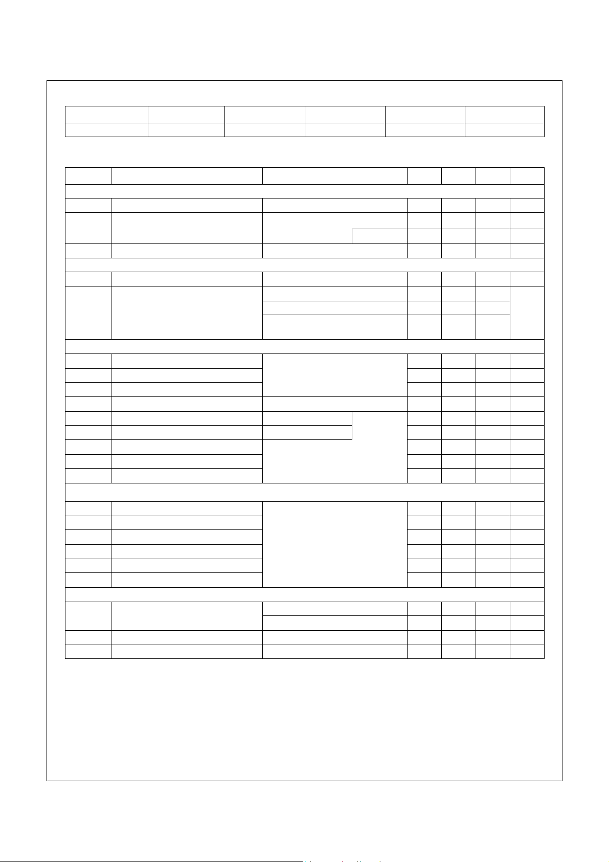
Symbol Parameter Conditions Min Typ Max Units
Off Characteristics
BV
DSS
I
DSS
I
GSS
On Characteristics
V
GS(th)
R
DS(on)
Dynamic Characteristics
C
iss
C
oss
C
rss
R
G
Q
g(tot)
Q
g(2)
Q
gs
Q
gs2
Q
gd
Switching Characteristics
t
ON
t
d(on)
t
r
t
d(off)
t
f
t
OFF
Drain-Source Diode Characteristics and Maximum Ratings
V
SD
t
rr
Q
RR
Drain to Source Breakdown Voltage VGS = 0V, ID = 250μA40----V
Zero Gate Voltage Drain Current
VDS = 32V
= 0 V
V
GS
T
= 150oC -- -- 250 μA
C
-- -- 1 μA
Gate to Body Leakage Current VGS = ±20V -- -- ±100 nA
Gate to Source Threshold Voltage VDS = VGS, ID = 250μA1--3V
= 4.5V, ID = 80A -- 1.88 2.4
V
Static Drain-Source On-Resistance
Input Capacitance
Output Capacitance -- 1840 2450 pF
GS
= 10V, ID = 80A -- 1.64 2.2
V
GS
= 10V, ID = 80A,
V
GS
T
= 175oC
C
-- 3.00 4.4
-- 18600 24740 pF
V
= 25V, VGS = 0V,
DS
f = 1.0MHz
mΩ
Reverse Transfer Capacitance -- 1400 2100 pF
Gate Resistance VGS = 0.5V, f = 1MHz -- 1.1 -- Ω
Total Gate Charge at 10V VGS = 0V to 10V
= 20V
Threshold Gate Charge VGS = 0V to 2V -- 32.5 -- nC
Gate to Source Gate Charge -- 49 -- nC
Gate Charge Threshold to Plateau -- 16.5 -- nC
V
DD
= 80A
I
D
= 1.0mA
I
g
-- 345 450 nC
Gate to Drain “Miller” Charge -- 74 -- nC
(V
= 10V)
GS
Turn-On Time
Turn-On Delay Time -- 43 95 ns
Rise Time -- 130 275 ns
= 20V,ID = 80A
V
DD
V
= 10V, R
GS
GEN
= 7Ω
-- 175 360 ns
Turn-Off Delay Time -- 435 875 ns
Fall Time -- 290 590 ns
Turn-Off Time -- 730 1470 ns
I
= 80A -- -- 1.25 V
Source to Drain Diode Voltage
SD
= 40A -- -- 1.0 V
I
SD
Reverse Recovery Time ISD = 75A, dISD/dt = 100A/μs--59--ns
Reverse Recovery Charge ISD = 75A, dISD/dt = 100A/μs--77--nC
®
MOSFET
NOTES:
1: Pulse width limited by maximum junction temperature.
2: Starting TJ = 25°C, L = 1mH, IAS = 58A, VDD = 36V, VGS = 10V.
FDP8440 Rev. A6
2 www.fairchildsemi.com

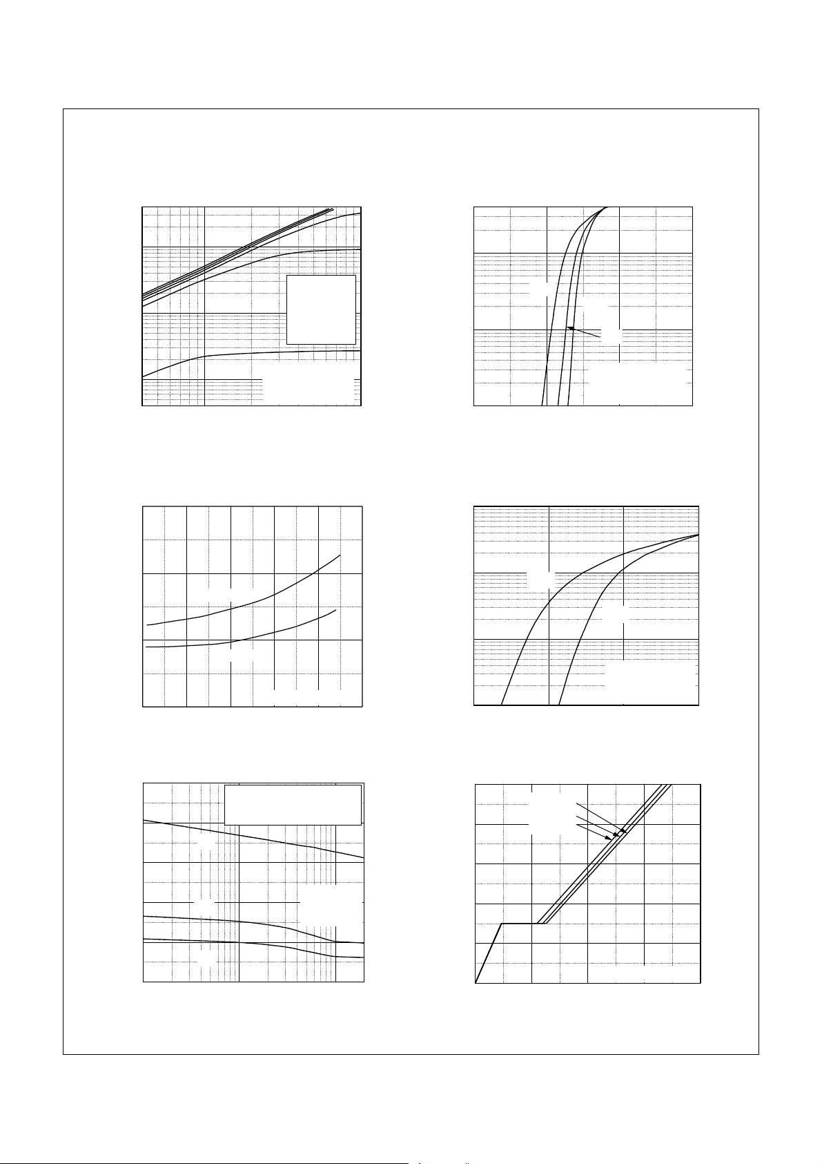
Typical Performance Characteristics
FDP8440 N-Channel PowerTrench
Figure 1. On-Region Characteristics Figure 2. Transfer Characteristics
400
100
10
,Drain Current[A]
D
I
1
0.4
0.04
0.1 1
VDS,Drain-Source Voltage[V]
* Notes :
1. 250
2. T
C
V
= 10.0 V
GS
7.0 V
5.0 V
3.5 V
3.0 V
2.5 V
μs Pulse Test
= 25oC
400
100
150oC
10
,Drain Current[A]
D
I
1
0246
VGS,Gate-Source Voltage[V]
-55oC
25oC
* Notes :
1. V
DS
2. 250
= 20V
μs Pulse Test
Figure 3. On-Resistance Variation vs. Figure 4. Body Diode Forward Voltage
Drain Current and Gate Voltage Variation vs. Source Current
and Temperatue
1.80
1.76
VGS = 4.5V
[mΩ],
DS(ON)
R
1.72
VGS = 10V
Drain-Source On-Resistance
* Note : TJ = 25oC
1.68
0 50 100 150 200 250
ID, Drain Current [A]
1000
100
150oC
25oC
10
, Reverse Drain Current [A]
S
I
1
0.3 0.6 0.9 1.2
Notes:
1. V
GS
2. 250
= 0V
μs Pulse Test
VSD, Body Diode Forward Voltage [V]
®
MOSFET
Figure 5. Capacitance Characteristics Figure 6. Gate Charge Characteristics
30000
24000
18000
12000
Capacitances [pF]
6000
FDP8440 Rev. A6
C
= Cgs + Cgd (Cds = shorted)
iss
C
= Cds + C
oss
C
rss
C
iss
= C
gd
gd
10
VDS = 25V
V
8
DS
V
DS
= 20V
= 15V
6
* Note:
1. V
C
oss
C
rss
0
-1
10
0
10
= 0V
GS
2. f = 1MHz
1
10
VDS, Drain-Source Voltage [V]
4
, Gate-Source Voltage [V]
GS
V
2
0
20
0 100 200 300 400
Qg, Total Gate Charge [nC]
* Note : ID = 80A
3 www.fairchildsemi.com
 Loading...