

查询FDB8030L供应商查询FDB8030L供应商
FDP8030L/FDB8030L
N-Channel Logic Level PowerTrench MOSFET
FDP8030L/FDB8030L
November 1999
General Description
This N-Channel Logic level MOSFET has been
designed specifically to improve the overall effici ency of
DC/DC converters using either synchronous or
conventional switching PWM controllers.
These MOSFETS feature faster switching and lower
gate charge than other MOSFETS with comparable
specifications.
R
DS(on)
The result is a MOSFET that is easy and safer to drive
(even at very high frequencies), and DC/DC power
supply designs with higher overall efficiency.
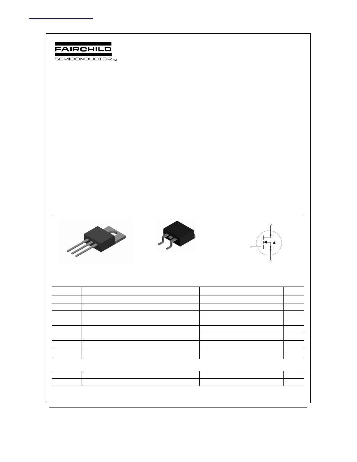
G
G
D
S
TO-220
FDP Series
S
Features
80 A, 30 V. R
•
Critical DC electrical parameters specified at
•
elevated temperature
Rugged internal source-drain diode can eliminate the
•
need for an external Zener diode transient
suppressor
High performance trench technology for extremely
•
low R
DS(ON)
175°C maximum junction temperature rating
•
D
= 0.0035 Ω @ VGS = 10 V
DS(ON)
= 0.0045 Ω @ VGS = 4.5 V
R
DS(ON)
G
D
TO-263AB
FDB Series
S
TA=25oC unless otherwise noted
Absolute Maximum Ratings
Symbol Parameter Ratings Units
V
DSS
V
GSS
I
D
P
D
TJ, T
T
L
STG
Drain-Source Voltage 30 V
Gate-Source Voltage
Drain Current – Continuous
– Pulsed
Total Power Dissipation @# TC = 25°C
Derate above 25°C
(Note 1)
(Note 1)
20
±
80 A
300
187 W
1.25
W°C
Operating and Storage Junction Temperature Range -65 to +175
Maximum lead temperature for soldering purposes,
275
1/8” from case for 5 seconds
Thermal Characteristics
R
JC
θ
R
JA
θ
1999 Fairchild Semiconductor Corpor ation
Thermal Resistance, Junction-to-Case 0.8
Thermal Resistance, Junction-to-Ambient 62.5
°
°
FDP8030L Rev C(W)
V
C
°
C
°
C/W
C/W
Electrical Characteristics
TA = 25°C unless otherwise noted
Symbol Parameter Test Conditions Min Typ Max Units
Drain-Source Avalanche Ratings
W
DSS
I
AR
Single Pulse Drain-Source
Avalanche Energy
Maximum Drain-Source Avalanche
Current
Off Characteristics
BV
DSS
BV
∆
T
∆
I
DSS
I
GSSF
I
GSSR
On Characteristics
V
GS(th)
GS(th)
V
∆
T
∆
R
DS(on)
I
D(on)
g
FS
Drain–Source Breakdown Voltage
Breakdown Voltage Temperature
DSS
Coefficient
J
Zero Gate Voltage Drain Current
Gate–Body Leakage, Forward
Gate–Body Leakage, Reverse
Gate Threshold Voltage
Gate Threshold Voltage
Temperature Coefficient
J
Static Drain–Source
On–Resistance
On–State Drain Current
Forward Transconductance
(Note 2)
Dynamic Characteristics
C
iss
C
oss
C
rss
Input Capacitance
Output Capacitance
Reverse Transfer Capacitance
(Note 1)
VDD = 20 V, ID = 80 A 1500 mJ
= 0 V, ID = 250 µA
V
GS
= 250 µA, Referenced to 25°C
I
D
= 24 V, VGS = 0 V 10
V
DS
= 20 V, VDS = 0 V 100 nA
V
GS
= –20 V VDS = 0 V –100 nA
V
GS
= VGS, ID = 250 µA
V
DS
I
= 250 µA, Referenced to 25°C
D
VGS = 10 V, ID = 80 A
=125°C
T
J
V
= 4.5 V, ID = 70 A 3.6 4.5
GS
= 10 V, VDS = 10 V 60 A
V
GS
= 10 V, ID = 80 A 170 S
V
DS
V
= 15 V, V
DS
GS
= 0 V,
f = 1.0 MHz
30 V
23
11.52 V
–5
3.1
4.0
10500 pF
2700 pF
1650 pF
80 A
mV/°C
mV/°C
3.5
5.6
A
µ
m
Ω
Switching Characteristics
t
D(on)
t
r
t
D (off)
t
f
Q
Q
Q
g
gs
gd
Turn–On Delay Time 20 35 ns
Turn–On Rise Time 185 225 ns
Turn–Off Delay Time 160 200 ns
Turn–Off Fall Time
Total Gate Charge 120 170 nC
Gate–Source Charge 27 nC
Gate–Drain Charge
(Note 2)
= 15 V, ID = 50 A,
V
DD
= 4.5 V, R
V
GS
= 10
R
V
I
D
Ω
GS
= 15 V,
DS
= 80 A, VGS = 5 V
GEN
Drain–Source Diode Characteristics and Maximum Ratings
I
S
I
SM
V
SD
Notes:
Pulse Test: Pulse Width < 300µs, Duty Cycle < 2.0%
1.
Maximum Continuous Drain–Source Diode Forward Current
Maximum Pulsed Drain-Source Diode Forward Current
Drain–Source Diode Forward Voltage VGS = 0 V, IS = 80 A
= 10
(Note 1)
(Note 1)
(Note 1)
Ω
200 240 ns
48 nC
80 A
300 A
11.3 V
FDP8030L Rev C(W)
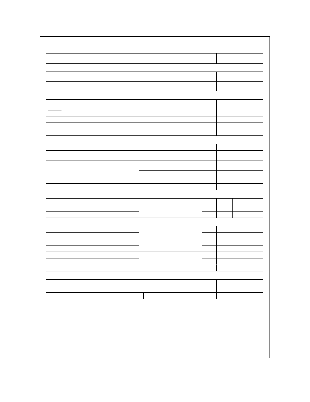
Typical Characteristics
FDP8030L/FDB8030L
100
4.5V
80
3.5V
60
40
3.0V
2.5V
20
D
I , DRAIN-SOURCE CURRENT (A)
0
0 0.5 1 1.5 2
V , DRAIN-SOURCE VOLTAGE (V)
DS
3
V = 2.5V
2.5
GS
2
1.5
DS(ON)
R , NORMALIZED
1
DRAIN-SOURCE ON-RESISTANCE
0.5
0 20406080100120
3.0V
3.5V
4.5V
I , DRAIN CURRENT (A)
D
6.0V
Figure 1. On-Region Characteristics. Figure 2. On-Resistance Variation with
Drain Current and Gate Voltage.
1.6
I = 80A
D
V = 10V
GS
1.4
1.2
1
DS(ON)
R , NORMALIZED
0.8
DRAIN-SOURCE ON-RESISTANCE
0.6
-50 -25 0 25 50 75 100 125 150
T , JUNCTION TEMPERATURE (°C)
J
0.01
0.009
0.008
0.007
0.006
0.005
0.004
0.003
, ON-RESISTANCE (OHM)
0.002
DS(ON)
R
0.001
0
2345678
V
, GATE TO SOURCE VOLT AGE ( V )
GS
TA = 125oC
TA = 25oC
10V
ID = 40A
Figure 3. On-Resistance Variation with
Temperature.
60
V = 10V
DS
50
40
T = -55°C
30
20
D
I , DRAIN CURRENT (A)
10
0
1234
A
25°C
125°C
V , GATE T O SOURCE VOLTAGE (V)
GS
Figure 4. On-Resistance Variation with
Gate-to-Source Voltage.
60
10
T = 125°C
1
0.1
0.01
0.001
S
I , REVERSE DRAIN CURRENT (A)
0.0001
0 0.2 0.4 0.6 0.8 1 1.2 1.4
A
25°C
-55°C
V , BODY DIODE FORWARD VOLTAG E (V)
SD
Figure 5. Transfer Characteristics. Figure 6. Body Diode Forward Voltage Variation
with Source Current and Temperature.
V = 0V
GS
FDP8030L Rev C(W)

Typical Characteristics
FDP8030L/FDB8030L
10
I = 80A
D
8
6
4
2
GS
V , GATE-SOURCE VOLTAGE (V)
0
0 40 80 120 160 200 240
Q , GATE CHARGE (nC)
g
V = 5V
DS
10V
15V
18000
10000
5000
2000
CAPACITANCE (pF)
1000
V = 0V
GS
500
0.1 0.5 1 2 5 10 30
V , DRAIN TO SOURCE VOLTAGE (V)
DS
Figure 7. Gate Charge Characteristics. Figure 8. Capacitance Characteristics.
600
300
100
50
20
10
5
D
I , DRAIN CURRENT (A)
2
1
0.5
0.3 1 3 5 10 20 30 50
im
L
DS(ON)
R
GS
V = 10V
SINGLE PULSE
R = 0.8 °C/W
JC
θ
T = 25 °C
C
it
V , DRAIN-SOURCE VOLTAGE (V)
DS
100µs
1ms
10ms
100ms
DC
5000
4000
3000
2000
POWER (W)
1000
0
0.1 0.3 1 3 10 30 100 300 1,000
SINGLE PULSE TIME (mSEC)
SINGLE PULSE
R = 0.8°C/W
θ
C
iss
C
oss
C
rss
JC
T = 25°C
C
Figure 9. Maximum Safe Operating Area. Figure 10. Single Pulse Maximum
Power Dissipation.
1
D = 0.5
0.5
0.3
0.2
0.2
0.1
0.1
0.05
0.05
0.03
0.02
r(t), NORMALIZED EFFECTIVE
TRANSIENT THERMAL RESISTANCE
0.005
0.02
0.01
Single Pulse
0.01 0.05 0.1 0.5 1 5 10 50 100 500 1000
t ,TIME (ms)
1
R (t) = r(t) * R
JC
θ
R = 0.8 °C/W
JC
θ
P(pk)
t
1
t
2
T - T = P * R (t)
CJ
Duty Cycle, D = t /t
JC
θ
JC
θ
1
2
Figure 11. Transient Thermal Response Curve.
Thermal characterization performed using the conditions described in Note 1c.
Transient thermal response will change depending on the circuit board design.
FDP8030L Rev C(W)

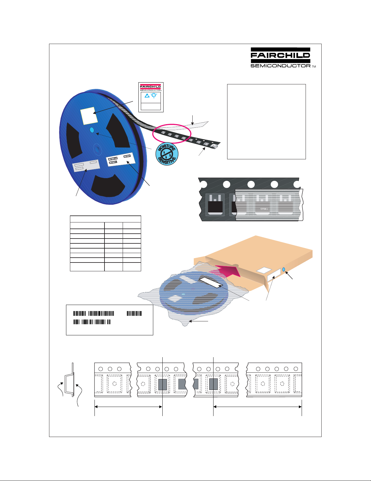
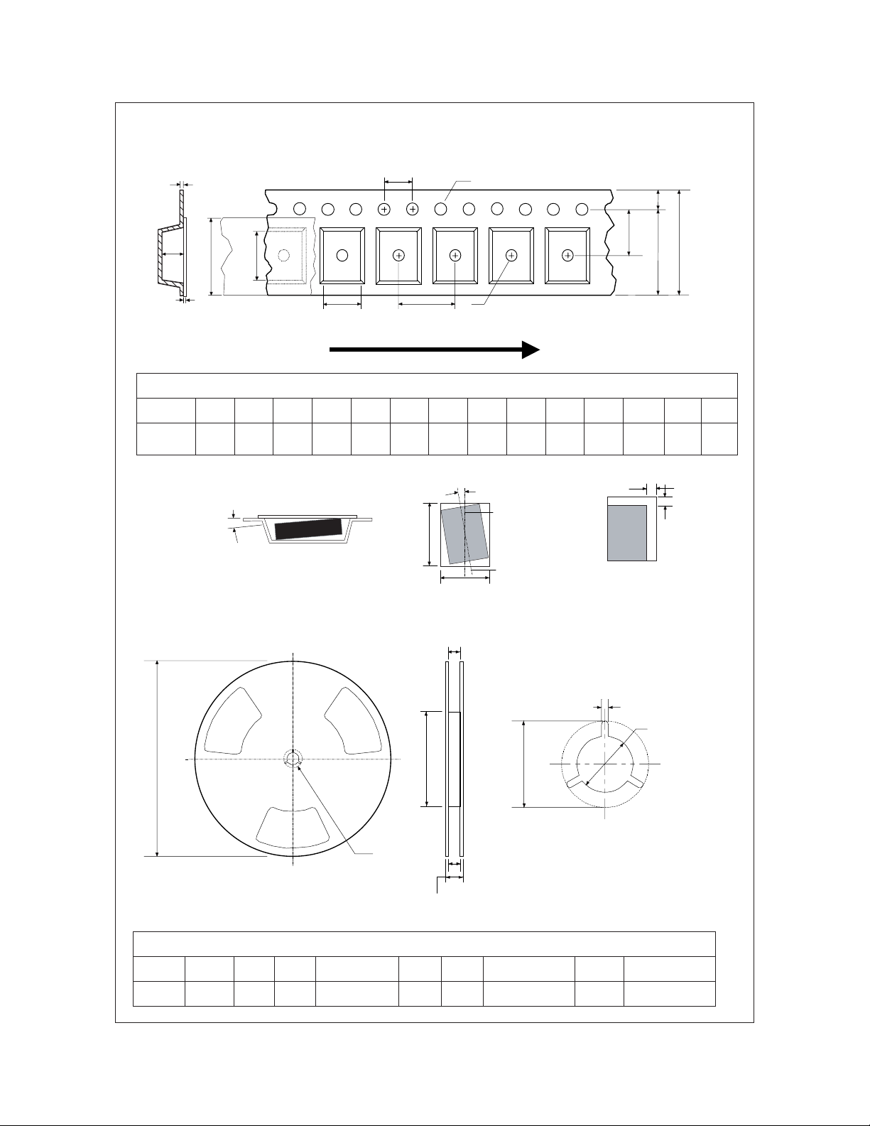
TO-220 Tape and Reel Data and Package Dimensions
TO-220 Tube Packing
Configuration: Figure 1.0
45 units per Tube
12 Tubes per Bag
530mm x 130mm x 83mm
2 bags per Box
Conduct ive Plastic Bag
Intermediate box
Packaging Description:
TO-220 par ts are shipped no rmally in tube. The tube is
made of PVC plas tic treated wi th anti -stati c agent .These
tubes in s tandard opt ion are placed in side a di ssipativ e
plastic bag, barcode labeled, and placed inside a box
made of r ecy cl able cor rug ate d pape r. On e bo x c ont ain s
tw o ba gs m ax im um (se e fi g. 1. 0). A nd on e or se ver al o f
these boxes ar e placed ins ide a labeled shipp ing box
wh ic h c o m es in d i f fer en t s i zes de pe ndi ng o n th e nu m be r
of parts shipped. The other option comes in bulk as
described in the Packagin g In fo rm atio n tab le. The un its in
this op tion ar e placed inside a s mall box laid w ith antistatic bu bble sheet. These smaller box es are indiv idually
labeled and plac ed inside a lar ger box (see fig. 3.0).
These larger or int ermediate boxes then w ill be placed
finally ins ide a labeled ship ping box whic h st ill co mes in
diff erent sizes depending on the num ber of units shipped.
TO-220 Packaging
Information: Figure 2.0
TO-220 Packaging Information
Packaging Option
Packaging type
Qty per Tube/Box
Box Dimension (mm)
Max qty per Box
Weight per unit (gm)
Note/Comments
Stan dard
(no fl ow code )
Rail/Tube
45
530x130x83
1,080
1.4378
S62Z
BULK
114x102x51
1,500
1.4378
TO-220 bulk Packing
Configuration: Figure 3.0
FSCINT L abel
300 units per
EO70 box
114mm x 102mm x 51mm
TO-220 Tube
Configuration: Figure 4.0
Note: All dim ensions are in inches
9852
9852
F
F
NDP4060L
NDP4060L
300
EO70 Immediate Box
9852
F
NDP4060L
9852
F
NDP4060L
9852
F
NDP4060L
9852
F
NDP4060L
Anti-static
Bubbl e Sheets
5 EO70 boxes per per
Interme di ate Box
9852
9852
F
NDP4060L
F
NDP4060L
20.000
+0.031
-0.065
F
NDP4060L
1080 units maximum
quantity per box
FSCINT L abel
0.123
+0.001
-0.003
9852
9852
F
NDP4060L
9852
F
NDP4060L
FSCINT Label sample
530mm x 130mm x 83mm
Intermediate box
FSCINT L abel
0.450
9852
F
NDP4060L
±.030
0.800
FAIRCHILD SEMICONDUCTOR CORPORAT ION
LOT:
CBVK741B019
NSID:
FDP7060
D/C1:
SPEC REV:
D9842
1500 units maximum
quantity per intermediate box
0.165
0.080
0.275
1.300
±.015
0.032
±.003
0.275
QA REV:
0.160
HTB:B
QTY:
1080
SPEC:
B2
(FSCINT)
August 1999, Rev. B

TO-220 Tape and Reel Data and Package Dimensions, continued
TO-220 (FS PKG Code 37)
1:1
Scale 1:1 on letter size paper
Dimensions shown below are in:
inches [millimeters]
Part Weight per unit (gram): 1.4378
September 1998, Rev. A
TO-263AB/D2PAK Tape and Reel Data and Package
Dimensions
TO-263AB/D2PAK Packaging
Configuration: Figure 1.0
ELECTROSTATIC
SENSITIVE DEVICES
DO NOT SHIP OR STORE NEAR STRONG ELECTROSTATIC
ELECTROMAGNETIC, MAGNETIC OR RADIOACTIVE FIELDS
TNR DATE
PT NUMBER
PEEL STRENGTH MIN ______________gms
Customized
Label
MAX _____________ gms
ESD Label
Moisture Sensitive
Antistatic Cover Tape
CAUTION
Label
F63TNR
Label
Static Dissipative
Embossed Car rier Tape
FDB603AL
F
9835
Packaging Description:
TO-263/D2PAK parts are shipped in tape. The carrier tape
is made from a dissipative (carbon filled) polycarbonate
resin. The cover tape is a multilayer film (Heat Activated
Adhesive in nature) primarily composed of polyester film,
adhesive layer, sealant, and anti-static sprayed agent.
These reeled parts in standard option are shipped with
800 unit s per 13" or 330cm di ameter reel. Th e reels are
dark blue in color and is made of polystyrene plastic (antistatic coated). This and some other options are further
described in the Packaging Information table.
These full reels are individually barcode labeled, dry
packed, and placed inside a standard intermediate box
(illus trated in fi gure 1.0) ma de of recycla ble corru gated
brown paper. One box c ontains one reel maximum. And
these boxes are placed inside a barcode labeled shipping
box which comes in different sizes depending on the
number of parts shipped.
FDB603AL
F
9835
FDB603AL
F
9835
FDB603AL
F
9835
TO-263AB/D2PAK Packaging Information
Packaging Option
Packaging type
Qty per Reel/Tube/Bag
Reel Size
Box Dimension (mm)
Max qty per Box
Weight per unit (gm)
Weight per Reel
Note/Comments
Standard
(no flow code)
TNR
13" Dia
359x359x57 530x130x83
1.4378 1.4378
1.6050 -
L86Z
Rail/Tube
800 45
800 1,080
-
F63TNR Label sample
LOT: CBVK741B019
FSID: FDB6320L
D/C1: D9842 QTY1: SPEC REV:
D/C2: QTY2: CPN:
QTY: 800
SPEC:
N/F: F (F63TNR)3
TO-263AB/D2PAK Tape Leader and Trailer
Configuration: Figure 2.0
TO-263AB/D2PAK Unit Orientation
359mm x 359mm x 57mm
Stand a r d In t e rm ed iate box
ESD Label
Moisture Sensitive
Label
F63TNR Label
DRYPACK Bag
Carrier Tape
Cover Tape
Trailer Tape
400mm minimum or
25 empty pockets
Components
Leader Tape
1520mm minimum or
95 empty pockets
September 1999, Rev. B
TO-263AB/D2PAK Tape and Reel Data and Package Dimensions, continued
TO-263AB/D2PAK Embossed Carrier Tape
Configuration: Figure 3.0
T
K0
Wc
Tc
B0
A0
P0
D0
P1
User Direction of Feed
Dimensions are in millimeter
E1
F
W
E2
D1
Pkg ty pe
T
O263AB/
2
D
PAK
(24mm)
Notes: A0, B0, and K0 dimensions are determined with respect to the EIA/Jedec RS-481
TO-263AB/D
A0 B0 W D0 D1 E 1 E2 F P1 P0 K0 T Wc Tc
10.60
15.80
24.0
1.55
1.60
1.75
22.25
+/-0.10
+/-0.10
+/-0.3
+/-0.05
+/-0.10
+/-0.10
11.50
min
+/-0.10
rotational and lateral movement requirements (see sketches A, B, and C).
10 deg maximum
B0
10 deg maximum component rotation
Sketch A (Side or Front Sectional View)
Component Rotation
2
PAK Reel Configuration:
A0
Sketch B (Top View)
Component Rotation
Figure 4.0
W1 Measured at Hub
Dim A
max
Dim N
16.0
+/-0.1
Typical
component
cavity
center line
Typical
component
center line
Dim A
Max
Dim D
min
4.0
+/-0.1
4.90
0.450
+/-0.150
21.0
+/-0.3
0.9mm
maximum
+/-0.10
0.9mm
maximum
Sketch C (Top View)
Component lateral movement
B Min
Dim C
0.06
+/-0.02
Tape Size
24mm 13" Dia
Reel
Option
DETAIL AA
13" Diameter Option
See detail AA
W2 max Measured at Hub
W3
Dimensions are in inches and millimeters
Dim A Dim B Dim C Dim D Dim N Dim W1 Dim W2 Dim W3 (LSL-USL)
13.00
0.059
1.5
512 +0.020/ -0.008
13 +0.5/-0.2
330
0.795
20.2
4.00
100
0.961 +0.078/-0.000
24.4 +2/0
1.197
30.4
0.941 – 0.1.079
23.9 – 27.4
August 1999, Rev. B

TO-263AB/D2PAK Tape and Reel Data and Package Dimensions, continued
TO-263AB/D2PAK (FS PKG Code 45)
1:1
Scale 1:1 on letter size paper
Dimensions shown below are in:
inches [millimeters]
Part Weight per unit (gram): 1.4378
August 1998, Rev. A

TRADEMARKS
The following are registered and unregistered trademarks Fairchild Semiconductor owns or is authorized to use and is
not intended to be an exhaustive list of all such trademarks.
ACEx™
CoolFET™
CROSSVOLT™
2
E
CMOS
TM
FACT™
FACT Quiet Series™
®
FAST
FASTr™
GTO™
HiSeC™
ISOPLANAR™
MICROWIRE™
POP™
PowerTrench
QFET™
QS™
Quiet Series™
SuperSOT™-3
SuperSOT™-6
SuperSOT™-8
SyncFET™
TinyLogic™
UHC™
VCX™
DISCLAIMER
FAIRCHILD SEMICONDUCTOR RESERVES THE RIGHT TO MAKE CHANGES WITHOUT FURTHER
NOTICE TO ANY PRODUCTS HEREIN TO IMPROVE RELIABILITY, FUNCTION OR DESIGN. FAIRCHILD
DOES NOT ASSUME ANY LIABILITY ARISING OUT OF THE APPLICA TION OR USE OF ANY PRODUCT
OR CIRCUIT DESCRIBED HEREIN; NEITHER DOES IT CONVEY ANY LICENSE UNDER ITS PATENT
RIGHTS, NOR THE RIGHTS OF OTHERS.
LIFE SUPPORT POLICY
FAIRCHILD’S PRODUCTS ARE NOT AUTHORIZED FOR USE AS CRITICAL COMPONENTS IN LIFE SUPPORT
DEVICES OR SYSTEMS WITHOUT THE EXPRESS WRITTEN APPROV AL OF FAIRCHILD SEMICONDUCTOR CORPORA TION.
As used herein:
1. Life support devices or systems are devices or
systems which, (a) are intended for surgical implant into
the body, or (b) support or sustain life, or (c) whose
failure to perform when properly used in accordance
with instructions for use provided in the labeling, can be
reasonably expected to result in significant injury to the
user.
2. A critical component is any component of a life
support device or system whose failure to perform can
be reasonably expected to cause the failure of the life
support device or system, or to affect its safety or
effectiveness.
PRODUCT STA TUS DEFINITIONS
Definition of Terms
Datasheet Identification Product Status Definition
Advance Information
Preliminary
No Identification Needed
Obsolete
Formative or
In Design
First Production
Full Production
Not In Production
This datasheet contains the design specifications for
product development. Specifications may change in
any manner without notice.
This datasheet contains preliminary data, and
supplementary data will be published at a later date.
Fairchild Semiconductor reserves the right to make
changes at any time without notice in order to improve
design.
This datasheet contains final specifications. Fairchild
Semiconductor reserves the right to make changes at
any time without notice in order to improve design.
This datasheet contains specifications on a product
that has been discontinued by Fairchild semiconductor.
The datasheet is printed for reference information only.
Rev. D
 Loading...