Fairchild FDP6021P, FDB6021P service manual

查询FDB6021P供应商查询FDB6021P供应商
FDP6021P/FDB6021P
20V P-Channel 1.8V Specified PowerTrench
FDP6021P/FDB6021P
April 2001
PRELIMINARY
MOSFET
General Description
This P-Channel power MOSFET uses Fairchild’s low
voltage PowerTrench process. It has been optimized for
power management applications .
Features
• –28 A, –20 V. R
R
R
= 30 mΩ @ VGS = 4.5 V
DS(ON)
= 40 mΩ @ VGS = 2.5 V
DS(ON)
= 65 mΩ @ VGS = 1.8 V
DS(ON)
Applications
• Battery management
• Load switch
• Voltage regulator
.
• Critical DC electric al parameters specified at
elevated temperature
• High performance trench te chnology for extremely
low R
• 175°C maximum junct i on temperature rating
D
DS(ON)
S
G
G
G
D
S
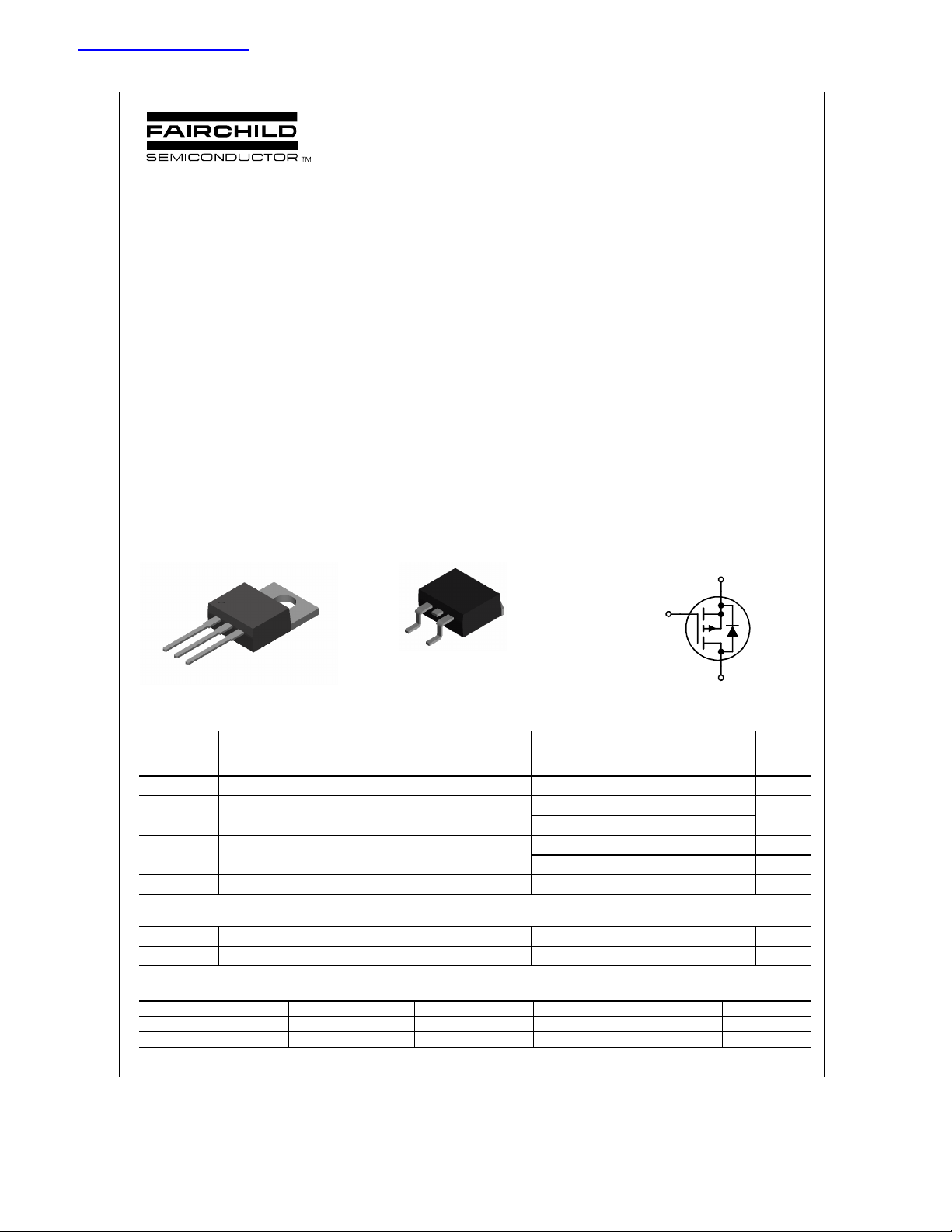
TO-220
FDP Series
Absolute Maximum Ratings T
S
o
=25
C unless otherwise noted
A
TO-263AB
FDB Series
D
Symbol Parameter Ratings Units
V
Drain-Source Voltage –20 V
DSS
V
Gate-Source Voltage
GSS
ID Drain Current – Continuous (Note 1) –28 A
– Pulsed (Note 1) –80
PD
TJ, T
STG
Total Power Dissipation @ T
Derate above 25°C
Operating and Storage Junction Temperature Range –65 to +175
= 25°C
C
± 8
37 W
0.25
V
W°C
°C
Thermal Characteristics
R
θJC
R
θJA
Thermal Resistance, Junction-to-Case
Thermal Resistance, Junction-to-Ambient
4
62.5
°C/W
°C/W
Package Marking and Ordering Information
Device Marking Device Reel Size Tape width Quantity
FDP6021P FDP6021P Tube n/a 45
FDB6021P FDB6021P 13” 24mm 800 units
2001 Fairchild Semiconductor Corporation
FDP6021P/FDB6021P Rev B ( W)

FDP6021P/FDB6021P
Electrical Characteristics T
= 25°C unless otherwise noted
A
Symbol Parameter Test Conditions Min Typ Max Units
Off Characteristics
BV
Drain–Source Breakdown Voltage
DSS
∆BVDSS
∆T
I
Zero Gate Voltage Drain Current VDS = –16 V, VGS = 0 V –1
DSS
I
GSSF
I
GSSR
Breakdown Voltage Temperature
Coefficient
J
Gate–Body Leakage, Forward VGS = 8 V, VDS = 0 V 100 nA
Gate–Body Leakage, Reverse VGS = –8 V VDS = 0 V –100 nA
V
= 0 V, ID = –250 µA
GS
= –250 µA,Referenced to 25°C
I
D
–20 V
–16
mV/°C
µA
On Characteristics (Note 2)
V
Gate Threshold Voltage
GS(th)
∆VGS(th)
∆TJ
R
DS(on)
Gate Threshold Voltage
Temperature Coefficient
Static Drain–Source
On–Resistance
I
On–S t ate Drain Current VGS = –4.5 V, VDS = –5 V –40 A
D(on)
V
= VGS, ID = –250 µA
DS
= –250 µA,Referenced to 25°C
I
D
VGS = –4.5 V, ID = –14 A
= –2.5 V, ID = –12 A
V
GS
V
= –1.8 V, ID = –10 A
GS
= –4.5V, ID = –14 A, TJ=125°C
V
GS
–0.4 –0.7 –1.5 V
3
24
31
50
30
30
40
65
42
mV/°C
mΩ
gFS Forward Transconductance VDS = –5 V, ID = –14 A 33 S
Dynamic Characteristics
C
Input Capacitance 1890 pF
iss
C
Output Capacitance 302 pF
oss
C
Reverse Transfer Capacitance
rss
= –10 V, V
V
DS
f = 1.0 MHz
= 0 V,
GS
124 pF
Switching Characteristics (Note 2)
t
Turn–On Delay Time 13 23 ns
d(on)
tr Turn–On Rise Time 10 20 ns
t
Turn–Off Delay Time 80 128 ns
d(off)
tf Turn–Off Fall Time
Qg Total Gate Charge 20 28 nC
Qgs Gate–Source Charge 4 nC
Qgd Gate–Drain Charge
= –10 V, ID = –1 A,
V
DD
= –4.5 V, R
V
GS
= –10 V, ID = –14 A,
V
DS
V
= –4.5 V
GS
GEN
= 6 Ω
50 80 ns
7 nC
Drain–Source Diode Characteristics and Maximum Ratings
IS Maximum Continuous Drain–Source Diode Forward Current –28 A
VSD Drain–Source Diode Forward
Voltage
Notes:
1. Pulse Test: Pulse Width < 300µs, Duty Cycle < 2.0%
2. TO-220 package is supplied in tube / rail @ 45 pieces per rail.
3. Calculated continuous current based on maximum allowable junction temperature. Actual maximum continuous current limited by package constraints to 75A
VGS = 0 V, IS = –14 A –0.9 –1.3 V
FDP6021P/FDB6021P Rev . B(W)
 Loading...