

FDP3651U
N-Channel PowerTrench
100V, 80A, 15mΩ
®
MOSFET
FDP3651U N-Channel PowerTrench
July 2006
Features
•r
•Q
• Low Miller Charge
• Low Q
• UIS Capability (Single Pulse/Repetitive Pulse)
MOSFET Maximum Ratings T
V
V
I
P
E
T
T
=13 mΩ(Typ.), VGS = 10V, ID = 40A
DS(on)
=49 nc(Typ.), VGS = 10 V
g(TOT)
Body Diode
rr
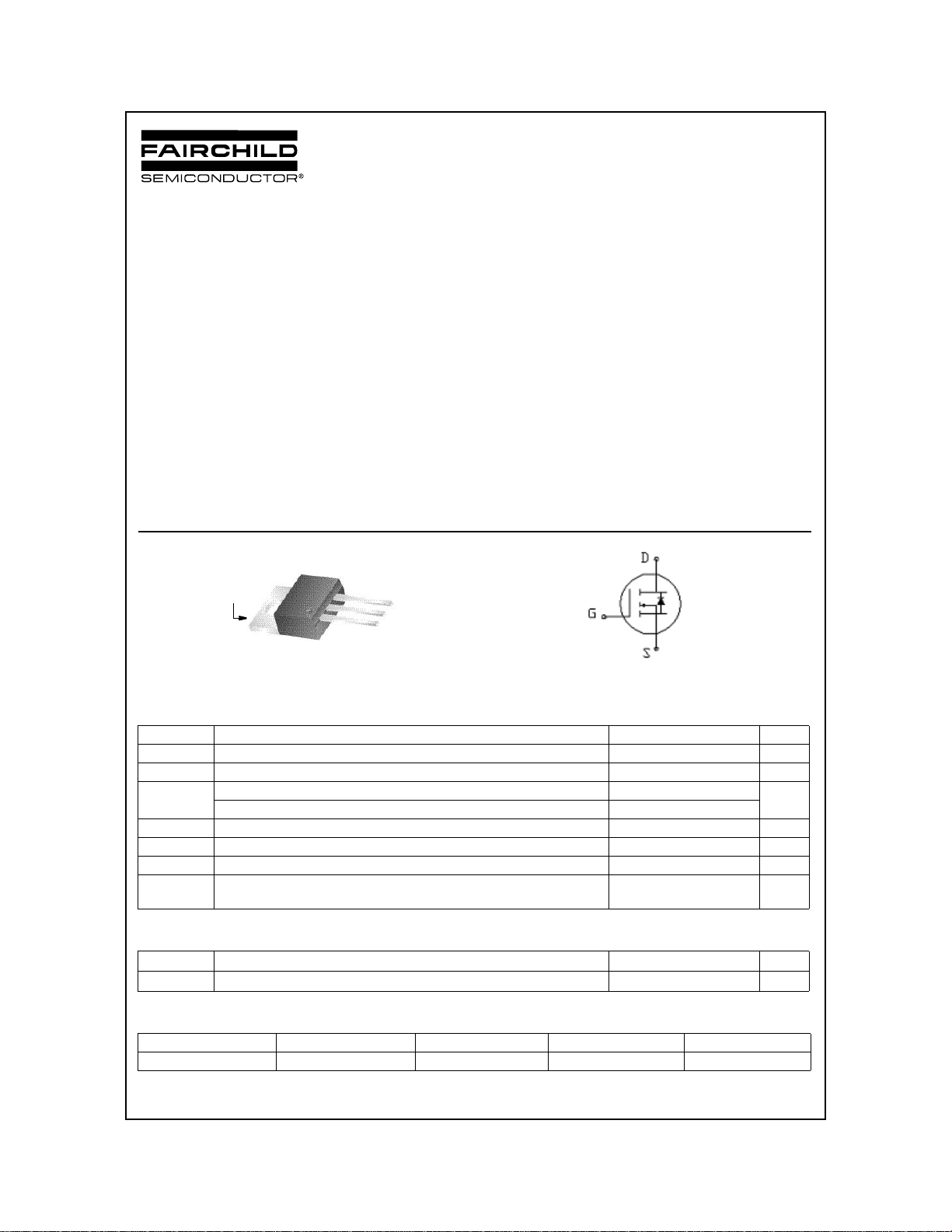
DRAIN
(FLANGE)
TO-220AB
FDP SERIES
Symbol Parameter Ratings Units
Drain to Source Voltage 100 V
Gate to Source Voltage ±20 V
Drain Current -Continuous 80
-Pulsed (Note 1)
Power Dissipation 255 W
Single Pulsed Avala nche Energy (Note 2) 266 mJ
Operating and Storage Temperature -55 to 175 °C
Maximum lead temperature soldering purposes,
1/8” from case for 5 seconds
D
DSS
GSS
D
AS
, T
J
L
STG
SOURCE
DRAIN
GATE
= 25°C unless otherwise noted
C
Applications
• DC/DC converters and Off-Line UPS
• Distributed Power Architectures and VRMs
• Primary Switch for 24V and 48V Systems
• High Voltage Synchronous Rectifier
320
300 °C
®
MOSFET
A
Thermal Characteristics
R
θJA
R
θJC
Thermal Resistance , Junction to Ambient 62 °C/W
Thermal Resistance , Junction to Case 0.59 °C/W
Package Marking and Ordering Information
Device Marking Device Reel Size Tape Width Quantity
FDP3651U FDP3651U Tube N/A 50 units
©2006 Fairchild Semiconductor Corporation
FDP3651U Rev. A
www.fairchildsemi.com1
Electrical Characteristics T
= 25°C unless otherwise noted
J
Symbol Parameter Test Conditions Min Typ Max Units
Off Characteristics
BV
I
DSS
I
GSS
DSS
Drain to Source Breakdown Voltage ID = 250µA, VGS = 0V 100 - - V
Zero Gate Voltage Drain Current
V
V
DS
GS
= 80V
= 0V
=150°C - - 250 µA
T
C
- - 1 µA
Gate to Source Leakage Current VGS = ±20V - - ±100 nA
On Characteristics
V
GS(th)
r
DS(on)
Gate to Source Threshold Voltage VGS = VDS, ID = -250µA 3.5 4.5 5.5 V
V
= 10V , ID = 80A - 15 18
GS
Drain to Source On Resistance
= 10V , ID = 40A - 13 15
GS
=10V, ID=40A,TJ=175oC - 32 37
V
GS
Dynamic Characteristics
C
iss
C
oss
C
rss
Q
g(TOT)
Q
g(TH)
Q
gs
Q
gd
Input Capacitance
Output Capacitance - 485 728 pF
Reverse Transfer Capacitance - 89 11 8 pF
= 25V,VGS = 0V
V
DS
f=1MHz
Total Gate Charge VGS = 0V to 10V
= 50V
V
Threshold Gate Charge VGS = 0V to 2V - 7 9.8 nC
Gate to Source Gate Charge - 23 - nC
DD
I
= 80A
D
- 4152 5522 pF
- 49 69 nC
Gate to Drain Charge - 16 - nC
FDP3651U N-Channel PowerTrench
mΩV
®
MOSFET
Resistive Switching Characteristics
t
(on)
t
d(on)
t
r
t
d(off)
t
f
t
(off)
Turn-On Time
Turn-On Delay Time - 15 27 ns
Rise Time - 16 29 ns
Turn-Off Delay Time - 32 52 ns
Fall Time - 14 26 ns
Turn-Off Time - - 78 ns
Drain-Source Diode Characteristics
V
SD
t
rr
Q
rr
Notes:
1. Pulse Test:Pulse Width<300us,Duty Cycle<2.0%
2. L=0.13mH, I
Source to Drain Diode Forward Voltage
Reverse Recovery Time
Reverse Recovery Charge - 202 303 nC
= 64A, VDD=50V, RG=25 Ω , Starting TJ=25oC
AS
- - 64 ns
V
= 50V, ID = 80A
DD
V
= 10V, RGS = 5.0Ω
GS
I
= 80A - 0.99 1.25 V
SD
= 40A - 0.88 1.0 V
I
SD
= 40 A, di/dt = 100A/µs
I
s
- 70 105 ns
FDP3651U Rev. A
www.fairchildsemi.com2

Typical Characteristics T
= 25°C unless otherwise noted
J
FDP3651U N-Channel PowerTrench
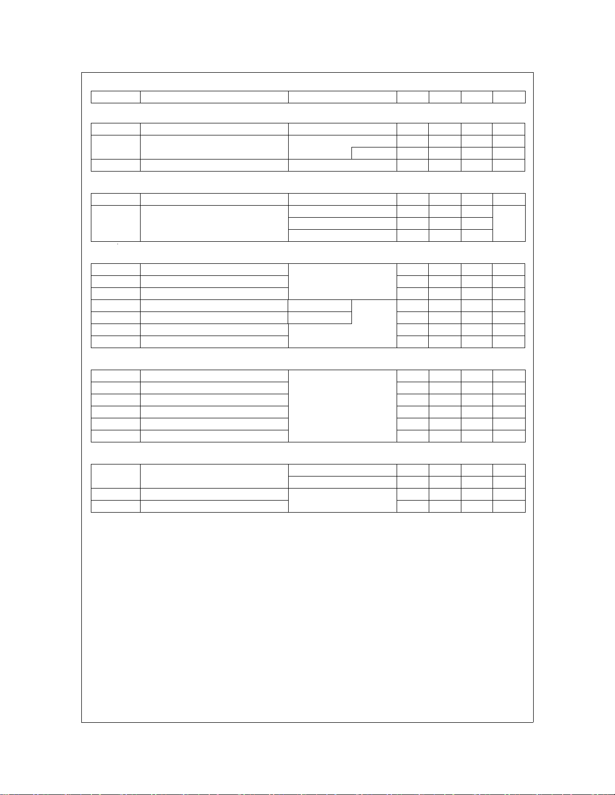
120
VGS = 20V
100
80
60
40
, DRAIN CURRENT (A)
D
I
20
0
012345
VDS, DRAIN TO SOURCE VOLTAGE (V)
PULSE DURATION = 80µs
DUTY CYCLE = 0.5%MAX
V
= 10V
GS
VGS = 8V
V
= 7V
GS
Figure 1. On Region Characteristics
2.8
ID = 80A
= 10V
V
GS
2.4
2.0
1.6
1.2
NORMALIZED
0.8
DRAIN-SOURCE ON-RESISTANCE
0.4
-80 -40 0 40 80 120 160 200
TJ, JUNCTION TEMPERATURE (oC)
5
V
= 7V
GS
4
3
2
NORMALIZED
1
0
DRAIN TO SOURCE ON-RESISTANCE
020406080100120
ID, DRAIN CURRENT(A)
Figure 2. Normalized
PULSE DURATION = 80µs
DUTY CYCLE = 0.5%MAX
VGS = 8V
VGS = 10V
V
GS
On-Resistance vs Drain
Current and Gate Voltage
60
50
40
30
20
, ON-RESISTANCE (mΩ)
10
DS(on)
R
0
8 101214161820
ID = 80A
VGS, GATE TO SOURCE VOLTAGE (V)
PULSE DURATION = 80µs
DUTY CYCLE = 0.5%MAX
TJ = 175oC
TJ = 25oC
= 20V
®
MOSFET
Figure 3.
120
100
80
60
40
, DRAIN CURRENT (A)
D
I
20
0
246810
Figure 5. Transfer Characteristics
FDP3651U Rev. A
Normalized On Resistance vs Junction
Temperature
PULSE DURATION = 80µs
DUTY CYCLE = 0.5%MAX
TJ = 175oC
TJ = 25oC
TJ = -55oC
VGS, GATE TO SOURCE VOLTAGE (V)
Figure 4.
On-Resistance vs Gate to Source
Voltage
1000
V
= 0V
GS
100
10
1
0.1
0.01
, REVERSE DRAIN CURRENT (A)
S
I
1E-3
0.0 0.2 0.4 0.6 0.8 1.0 1.2
Figure 6.
TJ = 175oC
TJ = 25oC
TJ = -55oC
VSD, BODY DIODE FORWARD VOLTAGE (V)
Source to Drain Diode Forward
Voltage vs Source Current
www.fairchildsemi.com3

0
Typical Characteristics T
= 25°C unless otherwise noted
J
FDP3651U N-Channel PowerTrench
10
8
VDD = 45V
VDD = 50V
V
= 55V
DD
6
4
2
, GATE TO SOURCE VOLTAGE(V)
GS
0
V
0 102030405060
Figure 7.
Qg, GATE CHARGE(nC)
Gate Charge Characteristics
100
10
TJ = 150oC
, AVALANCHE CURRENT(A)
AS
I
1
-3
-2
10
10
-1
10
tAV, TIME IN AVALANC HE (ms)
TJ = 25oC
0
1
10
10
2
10
3
10
10000
1000
C
iss
C
oss
C
rss
100
CAPACITANCE (pF)
Figure 8.
f = 1MHz
= 0V
V
GS
10
0.1 1 10 10
VDS, DRAIN TO SOURCE VOLTAGE (V)
Capacitance vs Drain to Source Voltage
100
PACKAGE MAY LIMIT
CURRENT IN THIS REGION
80
60
40
, DRAIN CURRENT (A)
20
D
I
0
25 50 75 100 125 150 175
VGS=10V
VGS=8V
TC, CASE TEMPERATURE (
®
MOSFET
o
C
)
Figure 9.
500
100
10
1
, DRAIN CURRENT (A)
D
I
0.1
110100
Figure 11.
FDP3651U Rev. A
Unclamped Inductive Switching
Capability
OPERATION IN THIS
AREA MAY BE
LIMITED BY R
SINGLE PULSE
T
Tc=25
DS(ON)
=MAX RATED
J
o
C
VDS, DRAIN TO SOURCE VOLTAGE (V)
10us
100us
1ms
10ms
DC
200
Figure 10.
5
10
4
10
3
10
), PEAK TRANSIENT POWER (W)
2
PK
10
P(
10
Maximum Continuous Drain Current vs
Ambient Temperature
VGS = 10V
SINGLE PULSE
-5
-4
10
t, PULSE WIDTH (s)
TC = 25oC
10-310
FOR TEMPERATURES
o
ABOVE 25
CURRENT AS FOLLOWS:
I = I
-2
25
C DERATE PEAK
175 Tc–
-----------------------
-1
10
Forward Bias Safe Operating Area Figure 12. Single Pulse Maximum Power
Dissipation
www.fairchildsemi.com4
150
0
10
1
10

FDP3651U N-Channel PowerTrench
Typical Characteristics T
2
DUTY CYCLE-DESCENDING ORDER
1
D = 0.5
0.2
0.1
θJA
0.1
0.05
0.02
0.01
-5
10
SINGLE PULSE
-4
10
Figure 13. Transient Thermal Response Curve
0.01
IMPEDANCE, Z
NORMALIZED THERMAL
1E-3
= 25°C unless otherwise noted
J
-3
10
-2
10
t, RECTANGULAR PULSE DURATION(s)
NOTES:
DUTY FACTOR: D = t1/t
PEAK TJ = PDM x Z
-1
10
P
DM
t
1
t
2
2
x R
+ T
θJc
θJc
c
0
10
1
10
®
MOSFET
FDP3651U Rev. A
www.fairchildsemi.com5

FAIRCHILD SEMICONDUCTOR TRADEMARKS
The following are registered and unregistered trademarks Fairchild Semiconductor owns or is authorized to use and is not
intended to be an exhaustive list of all such trademarks.
ACEx™
ActiveArray™
Bottomless™
Build it Now™
CoolFET™
CROSSVOLT™
DOME™
EcoSPARK™
2
E
CMOS™
EnSigna™
®
FACT
®
FAST
FASTr™
FPS™
FRFET™
FACT Quiet Series™
GlobalOptoisolator™
GTO™
HiSeC™
2
C™
I
i-Lo™
ImpliedDisconnect™
IntelliMAX™
ISOPLANAR™
LittleFET™
MICROCOUPLER™
MicroFET™
MicroPak™
MICROWIRE™
MSX™
MSXPro™
Across the board. Around the world.™
The Power Franchise
®
OCX™
OCXPro™
OPTOLOGIC
®
OPTOPLANAR™
PACMAN™
POP™
Power247™
PowerEdge™
PowerSaver™
PowerTrench
QFET
®
®
QS™
QT Optoelectronics™
Quiet Series™
RapidConfigure™
RapidConnect™
µSerDes™
ScalarPump™
SILENT SWITCHER
SMART START™
SPM™
Stealth™
SuperFET™
SuperSOT™-3
SuperSOT™-6
SuperSOT™-8
SyncFET™
TCM™
TinyBoost™
TinyBuck™
TinyPWM™
TinyPower™
TinyLogic
®
TINYOPTO™
TruTranslation™
®
UHC
Programmable Active Droop™
DISCLAIMER
FAIRCHILD SEMICONDUCTOR RESERVES THE RIGHT TO MAKE CHANGES WITHOUT FURTHER NOTICE TO ANY PRODUCTS
HEREIN TO IMPROVE RELIABILITY, FUNCTION, OR DESIGN. FAIRCHILD DOES NOT ASSUME ANY LIABILITY ARISING OUT OF THE
APPLICATION OR USE OF ANY PRODUCT OR CIRCUIT DESCRIBED HEREIN; NEITHER DOES IT CONVEY ANY LICENSE UNDER
ITS PATENT RIGHTS, NOR THE RIGHTS OF OTHERS. THESE SPECIFICATIONS DO NOT EXPAND THE TERMS OF FAIRCHILD’S
WORLDWIDE TERMS AND CONDITIONS, SPECIFICALLY THE WARRANTY THEREIN, WHICH COVERS THESE PRODUCTS.
®
UniFET™
VCX™
Wire™
LIFE SUPPORT POLICY
FAIRCHILD’S PRODUCTS ARE NOT AUTHORIZED FOR USE AS CRITICAL COMPONENTS IN LIFE SUPPORT DEVICES OR
SYSTEMS WITHOUT THE EXPRESS WRITTEN APPROVAL OF FAIRCHILD SEMICONDUCTOR CORPORATION.
As used herein:
1. Life support devices or systems are devices or systems which,
(a) are intended for surgical implant into the body, or (b) support or
sustain life, or (c) whose failure to perform when properly used in
accordance with instructions for use provided in the labeling, can be
reasonably expected to result in significant injury to the user.
2. A critical component is any component of a life support device or
system whose failure to perform can be reasonably expected to
cause the failure of the life support device or system, or to affect its
safety or effectiveness.
PRODUCT STATUS DEFINITIONS
Definition of Terms
Datasheet Identification Pr od u ct S ta t us Definition
Advance Information Formative or In Design This datasheet contains the design specifications for
Preliminary First Production This datasheet contains preliminary data, and
No Identification Needed Full Production This datasheet contains final specifications. Fairchild
Obsolete Not In Production This datasheet contains specifications on a product
product development. Specifications may change in
any manner without notice.
supplementary data will be published at a later date.
Fairchild Semiconductor reserves the right to make
changes at any time without notice to improve
design.
Semiconductor reserves the right to make changes at
any time without notice to improve design.
that has been discontinued by Fairchild semiconductor.
The datasheet is printed for reference information only.
Rev. I22
 Loading...