

Fairchild FDP22N50N service manual
FDP22N50N
N-Channel MOSFET
500V, 22A, 0.22Ω
FDP22N50N N-Channel MOSFET
April 2009
TM
UniFET
Features
•R
• Low gate charge ( Typ. 49nC)
• Low C
• Fast switching
• 100% avalanche tested
• Improve dv/dt capability
• RoHS compliant
MOSFET Maximum Ratings T
V
DSS
V
GSS
I
D
I
DM
E
AS
I
AR
E
AR
dv/dt Peak Diode Recovery dv/dt (Note 3) 10 V/ns
P
D
, T
T
J
T
L
*Drain current limited by maximum junction temperature
= 0.185Ω ( Typ.)@ VGS = 10V, ID = 11A
DS(on)
( Typ. 24pF)
rss
G
D
S
Symbol Parameter FDP22N50N Units
Drain to Source Voltage 500 V
Gate to Source Voltage ±30 V
D r a i n C urrent
Drain Current - Pulsed (Note 1) 88 A
Single Pulsed Avalanche Energy (Note 2) 1000 mJ
Avalanche Current (Note 1) 22 A
Repetitive Avalanche Energy (Note 1) 31.25 mJ
Power Dissipation
STG
Operating and Storage Temperature Range -55 to +150
Maximum Lead Temperature for Soldering Purpose,
1/8” from Case for 5 Seconds
TO-220
FDP Series
C
= 25oC unless otherwise noted
-Continuous (T
-Continuous (T
(T
= 25oC) 312.5 W
C
- Derate above 25
Description
These N-Channel enhancement mode power field effect
transistors are produced using Fairchild’s proprietary, planar
stripe, DMOS technology.
This advanced technology has been especially tailored to minimize on-state resistance, provide superior switching performance, and withstand high energy pulse in the avalanche and
commutation mode. These devices are well suited for high
efficient switching mode power supplies and active power factor
correction.
D
G
S
= 25oC) 22
C
= 100oC) 13.2
C
o
C2.5W/
300
o
o
Thermal Characteristics
Symbol Parameter FDP22N50N Units
R
θJC
θCS
R
θJA
Thermal Resistance, Junction to Case 0.4
Thermal Resistance, Case to Sink Typ. 0.5
Thermal Resistance, Junction to Ambient 62.5
o
C/WR
A
o
C
C
C
©2009 Fairchild Semiconductor Corporation
FDP22N50N Rev. A
www.fairchildsemi.com1
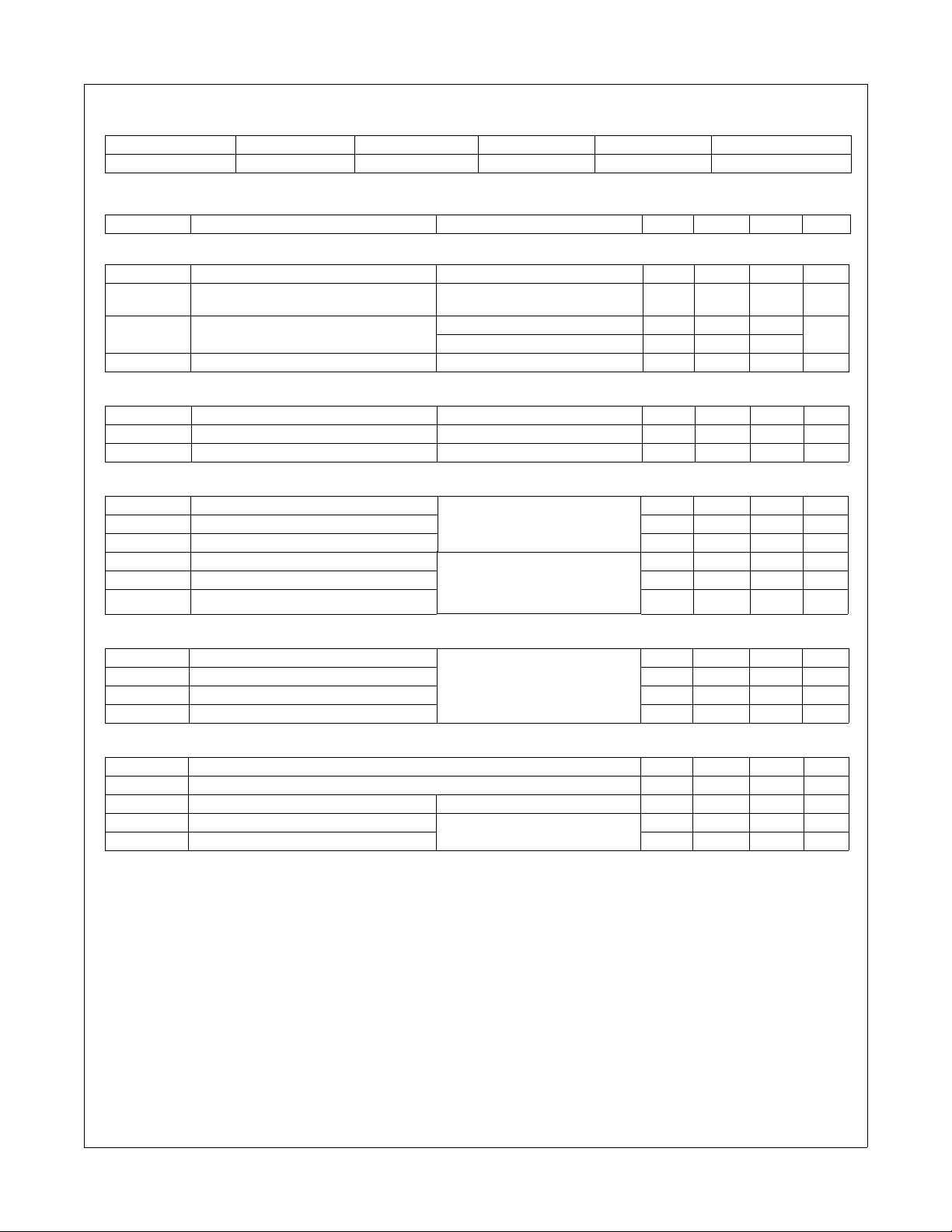
Package Marking and Ordering Information
Device Marking Device Package Reel Size Tape Width Quantity
FDP22N50N
FDP22N50N TO-220 - - 50
FDP22N50N N-Channel MOSFET
Electrical Characteristics T
= 25oC unless otherwise noted
C
Symbol Parameter Test Conditions Min. Typ. Max. Units
Off Characteristics
BV
DSS
∆BV
/ ∆T
I
DSS
I
GSS
DSS
J
Drain to Source Breakdown Voltage ID = 250µA, VGS = 0V, 500 - - V
Breakdown Voltage Temperature
Coefficient
Zero Gate Voltage Drain Current
Gate to Body Leakage Current VGS = ±30V, V
I
= 250µA, Referenced to 25oC - 0.45 - V/oC
D
V
= 500V, V
DS
= 400V, TC = 125oC--10
V
DS
= 0V - - 1
GS
= 0V - - ±100 nA
DS
On Characteristics
V
GS(th)
R
DS(on)
g
FS
Gate Threshold Voltage VGS = VDS, ID = 250µA3.0-5.0V
Static Drain to Source On Resistance VGS = 10V, ID = 11A - 0.185 0.22 Ω
Forward Transconductance VDS = 20V, ID = 11A - 24.4 - S
Dynamic Characteristics
C
C
C
Q
Q
Q
iss
oss
rss
g(tot)
gs
gd
Input Capacitance
Output Capacitance - 351 460 pF
Reverse Transfer Capacitance - 24 50 pF
Total Gate Charge at 10V
Gate to Source Gate Charge - 15 - nC
Gate to Drain “Miller” Charge - 19 - nC
Switching Characteristics
t
d(on)
t
r
t
d(off)
t
f
Turn-On Delay Time
Turn-On Rise Time - 50 110 ns
Turn-Off Delay Time - 48 110 ns
Turn-Off Fall Time - 35 80 ns
= 25V, VGS = 0V
V
DS
f = 1MHz
V
= 400V, ID = 22A
DS
V
= 10V
GS
(Note 4)
= 250V, ID = 22A
V
DD
R
= 4.7Ω
G
(Note 4)
- 2456 3200 pF
-4965nC
-2255ns
µA
Drain-Source Diode Characteristics
I
S
I
SM
V
SD
t
rr
Q
rr
Notes:
1. Repetitive Rating: Pulse width limited by maximum junction temperature
2. L = 4.1mH, I
≤ 22A, di/dt ≤ 200A/µs, VDD ≤ BV
3. I
SD
4. Essentially Independent of Operating Temperature Typical Characteristics
FDP22N50N Rev. A
Maximum Continuous Drain to Source Diode Forward Current - - 22 A
Maximum Pulsed Drain to Source Diode Forward Current - - 88 A
Drain to Source Diode Forward Voltage V
Reverse Recovery Time
Reverse Recovery Charge - 6.5 - µC
= 22A, VDD = 50V, RG = 25Ω, Starting TJ = 25°C
AS
, Starting TJ = 25°C
DSS
= 0V, I
GS
V
= 0V, I
GS
dI
/dt = 100A/µs
F
= 22A - - 1.4 V
SD
= 22A
SD
2
- 472 - ns
www.fairchildsemi.com
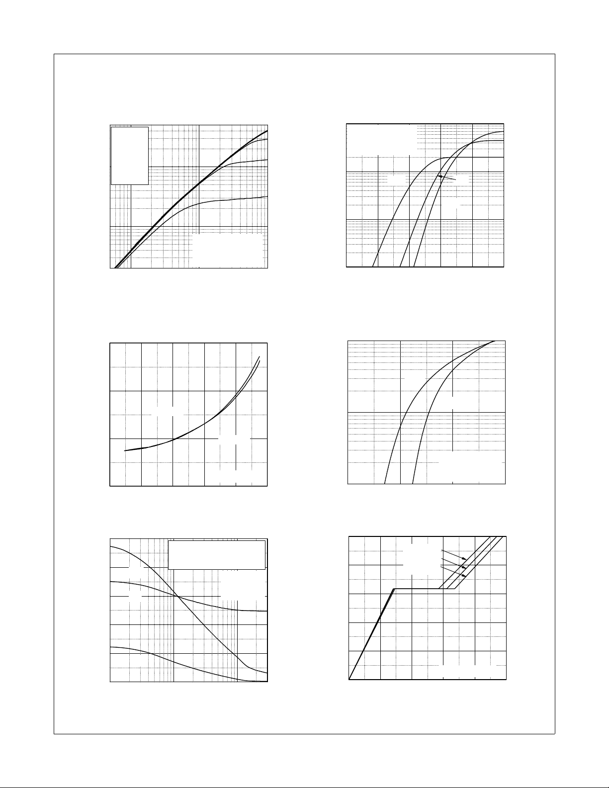
Typical Performance Characteristics
FDP22N50N N-Channel MOSFET
Figure 1. On-Region Characteristics Figure 2. Transfer Characteristics
50
V
= 15.0V
GS
10.0V
8.0 V
7.0 V
6.5 V
10
6.0 V
5.5 V
,Drain Current[A]
D
1
I
0.2
0.1 1 10
0.05
VDS,Drain-Source Voltage[V]
*Notes:
1. 250
2. T
µs Pulse Test
= 25oC
C
100
*Notes:
= 20V
1. V
DS
2. 250
µs Pulse Test
10
150oC
1
,Drain Current[A]
D
I
0.1
345678
25oC
-55oC
VGS,Gate-Source Voltage[V]
Figure 3. On-Resistance Variation vs. Figure 4. Body Diode Forward Voltage
Drain Current and Gate Voltage Variation vs. Source Current
and Temperature
0.30
0.25
[Ω],
DS(ON)
R
0.20
VGS = 10V
100
150oC
25oC
VGS = 20V
10
Drain-Source On-Resistance
0.15
0 1020304050
Figure 5. Capacitance Characteristics Figure 6. Gate Charge Characteristics
5000
4000
3000
2000
Capacitances [pF]
1000
0
0.1 1 10
FDP22N50N Rev. A
*Note: TJ = 25oC
ID, Drain Current [A]
C
= Cgs + Cgd (Cds = shorted)
iss
C
= Cds + C
oss
C
C
oss
C
iss
C
rss
rss
= C
gd
gd
VDS, Drain-Source Voltage [V ]
*Note:
= 0V
1. V
GS
2. f = 1MH z
, Reverse Drain Current [A]
S
I
1
0.2 0.6 1.0 1.4
*Notes:
1. VGS = 0V
2. 250
µs Pulse Test
VSD, Body Diode Forward Voltage [V]
10
VDS = 100V
V
= 250V
8
V
DS
= 400V
DS
6
, Gate-Source Voltage [V]
GS
V
4
2
*Note: ID = 22A
0
30
0 1020304050
Qg, Total G a te C harge [nC]
3
www.fairchildsemi.com
 Loading...