

现货库存、技术资料、百科信息、热点资讯,精彩尽在鼎好!
tm
FDN5632N_F085
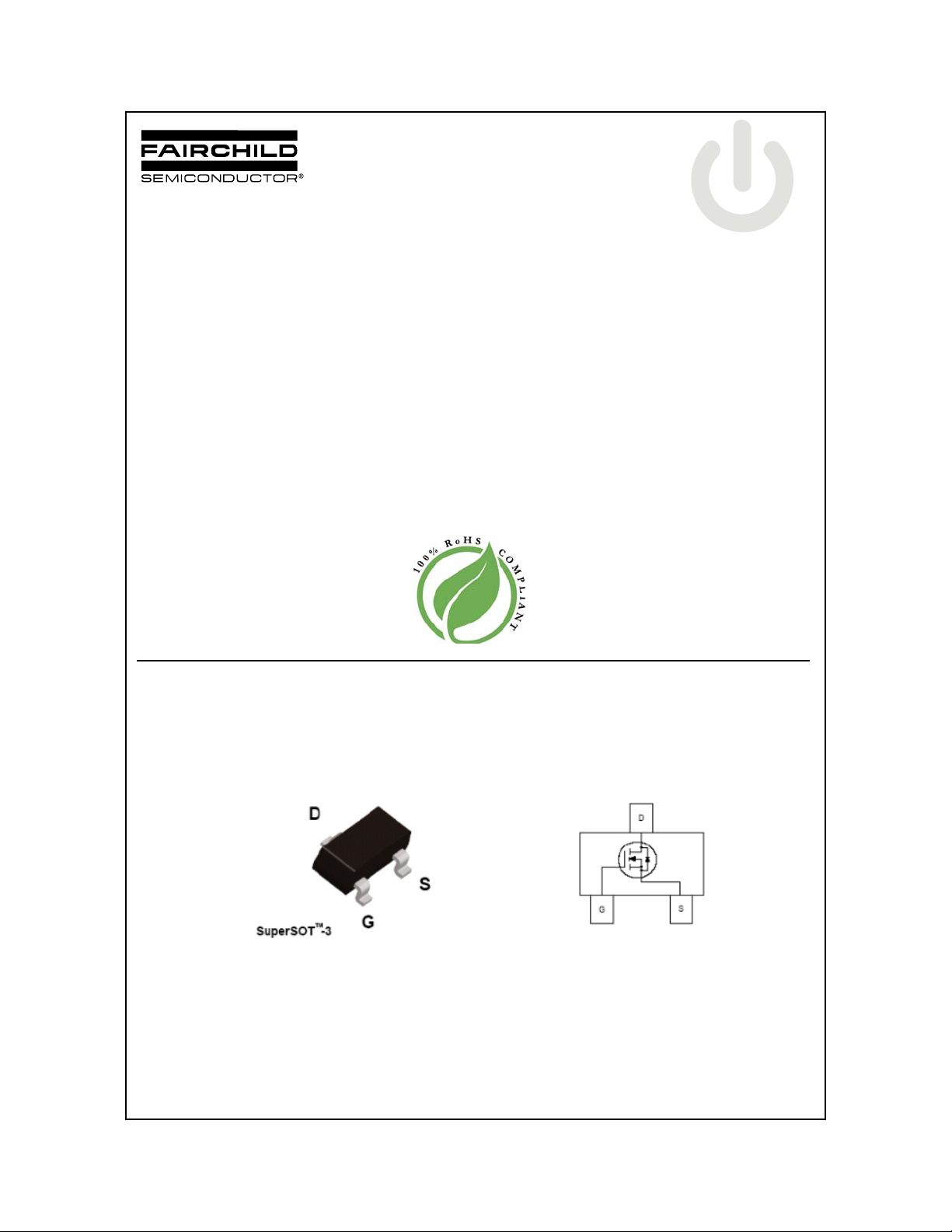
N-Channel Logic Level PowerTrench® MOSFET
60V, 1.6A, 98mΩ
FDN5632N_F085 N-Channel Logic Level PowerTrench
September 2008
Features
R
R
Typ Q
Low Miller Charge
Qualified to AEC Q101
RoHS Compliant
DS(on)
DS(on)
= 98mΩ at V
= 82mΩ at V
= 9.2nC at VGS = 10V
g(TOT)
GS
GS
= 4.5V, I
= 10V, I
= 1.6A
D
= 1.7A
D
Applications
DC/DC converter
Motor Drives
®
MOSFET
©2008 Fairchild Semiconductor Corporation
FDN5632N_F085 Rev. A (W)
www.fairchildsemi.com1
MOSFET Maximum Ratings T
= 25°C unless otherwise noted
A
Symbol Parameter Ratings Units
V
DSS
V
GS
I
D
P
D
T
J
Drain to Source Voltage 60 V
Gate to Source Voltage ±20 V
Drain Current Continuous (V
= 10V) 1.7
GS
Pulsed 10
Power Dissipation 1.1 W
, T
Operating and Storage Temperature -55 to +150
STG
Thermal Characteristics
FDN5632N_F085 N-Channel Logic Level PowerTrench
A
o
C
R
θJC
R
θJA
Thermal Resistance Junction to Case 75
Thermal Resistance Junction to Ambient TO-252, 1in2 copper pad area 111
o
o
Package Marking and Ordering Information
Device Marking Device Package Reel Size Tape Width Quantity
5632 FDN5632N_F085 SSOT3 7” 8mm 3000 units
Electrical Characteristics T
Symbol Parameter Test Conditions Min Typ Max Units
Off Characteristics
B
VDSS
I
DSS
I
GSS
On Characteristics
V
GS(th)
r
DS(on)
Drain to Source Breakdown Voltage ID = 250µA, VGS = 0V 60 - - V
Zero Gate Voltage Drain Current
Gate to Source Leakage Current VGS = ±20V - - ±100 nA
Gate to Source Threshold Voltage VGS = VDS, ID = 250µA12.03V
Drain to Source On Resistance
= 25°C unless otherwise noted
A
V
= 48V, - - 1
DS
= 0V TA = 125oC - - 250
V
GS
= 1.7A, VGS= 10V - 57 82
I
D
I
= 1.6A, VGS= 6V - 62 88
D
= 1.6A, VGS= 4.5V 70 98
I
D
= 1.7A, VGS= 10V,
I
D
T
= 150oC
A
-107135
C/W
C/W
µA
mΩ
®
MOSFET
Dynamic Characteristics
C
iss
C
oss
C
rss
R
G
Q
g(TOT)
Q
gs
Q
gd
Input Capacitance
Output Capacitance - 60 - pF
Reverse Transfer Capacitance - 30 - pF
= 15V, VGS = 0V,
V
DS
f = 1MHz
Gate Resistance f = 1MHz - 1.4 - Ω
Total Gate Charge at 10V VGS = 0 to 10V
Gate to Source Gate Charge
Gate to Drain “Miller“ Charge - 1.4 - nC
FDN5632N_F085 Rev. A (W) www.fairchildsemi.com2
V
DD
I
D
= 20V
= 1.7A
- 475 - pF
- 9.2 12 nC
-1.5-nC
FDN5632N_F085 N-Channel Logic Level PowerTrench
Electrical Characteristics T
= 25oC unless otherwise noted
A
Symbol Parameter Test Conditions Min Typ Max Units
Switching Characteristics
t
on
t
d(on)
t
r
t
d(off)
t
f
t
off
Turn-On Time
Turn-On Delay Time - 15 - ns
Rise Time - 1.7 - ns
Turn-Off Delay Time - 5.2 - ns
Fall Time - 1.3 - ns
Turn-Off Time - - 12.9 ns
Drain-Source Diode Characteristics
V
SD
t
rr
Q
rr
Source to Drain Diode Voltage
Reverse Recovery Time
Reverse Recovery Charge - 7.9 10.3 nC
= 30V, ID = 1.0A
V
DD
V
= 10V, R
GS
I
= 1.7A - 0.8 1.25
SD
= 0.85A - 0.8 1.0
I
SD
= 1.7A, dISD/dt = 100A/µs
I
SD
GEN
= 6Ω
- - 30 ns
- 16.0 21 ns
V
®
MOSFET
This product has been designed to meet the extreme test conditions and environment demanded by the automotive industry. For
All Fairchild Semiconductor products are manufactured, assembled and tested under ISO9000 and QS9000 quality systems
FDN5632N_F085 Rev. A (W) www.fairchildsemi.com3
a copy of the requirements, see AEC Q101 at: http://www.aecouncil.com/
certification.

Typical Characteristics
FDN5632N_F085 N-Channel Logic Level PowerTrench
1.2
1.0
0.8
0.6
0.4
0.2
POWER DISSIPATION MULTIPLIER
0.0
0 25 50 75 100 125 150
TA, AMBIENT TEMPERATURE(oC)
Figure 1. Normalized Power Dissipation vs
Ambient Temperature
2
DUTY CYCLE - DESCENDING ORDER
1
D = 0.50
0.1
0.20
0.10
0.05
0.02
0.01
SINGLE PULSE
R
= 111oC / W
θJA
-3
10
-2
10
-1
10
t, RECTANGULAR PULSE DURATION(s)
Figure 3.
Normalized Maximum Transient Thermal Impedance
θJA
IMPEDANCE, Z
NORMALIZED THERMAL
0.01
3
CURRENT LIMITED
BY PACKAGE
2
VGS = 10V
1
, DRAIN CURRENT (A)
D
I
R
θ
JA
= 111oC/W
VGS = 4.5V
0
25 50 75 100 125 150
TA, AMBIENT TEMPERATURE
o
(
C
Figure 2. Maximum Continuous Drain Current vs
Ambient Temperature
P
DM
t
1
NOTES:
DUTY FACTOR: D = t1/t
PEAK TJ = PDM x Z
0
10
1
10
2
10
θJA
x R
2
+ T
θJA
3
10
)
®
MOSFET
t
2
A
4
10
100
VGS = 10V
10
, PEAK CURRENT (A)
DM
I
1
-3
10
SINGLE PULSE
R
= 111oC / W
θ
JA
-2
10
-1
10
11010210
t, RECTANGULAR PULSE DURATION(s)
Figure 4. Peak Current Capability
FDN5632N_F085 Rev. A (W) www.fairchildsemi.com4
TC = 25oC
FOR TEMPERATURES
o
ABOVE 25
CURRENT AS FOLLOWS:
I = I
25
C DERATE PEAK
150 - T
125
3
C
4
10

Typical Characteristics
FDN5632N_F085 N-Channel Logic Level PowerTrench
30
10
100us
1
1ms
0.1
, DRAIN CURRENT (A)
D
I
0.01
OPERATION IN THIS
AREA MA Y B E
LIMITED BY
0.001
0.01 0.1 1 10 100 300
r
DS(on)
SINGLE PULSE
T
= MAX RATED
J
o
T
= 25
C
A
10ms
100ms
1s
DC
VDS, DRAIN TO SOURCE VOLTAGE (V)
Figure 5.
12
, DRAIN CURRENT (A)
D
I
Forward Bias Safe Operating Area
VGS = 10V
VGS = 6V
9
6
3
0
01234
VGS = 5V
VGS = 4.5V
VGS = 4V
PULSE DURATION = 80µs
DUTY CYCLE = 0.5% MAX
VGS = 3.5V
V
= 3V
GS
VDS, DRAIN TO SOURCE VOLTA GE (V)
12
PULSE DURATION = 80µs
DUTY CYCLE = 0.5% MAX
= 5V
V
9
DD
6
TJ = 25oC
3
, DRAIN CURRENT (A)
D
I
0
012345
TJ = 150oC
TJ = -55oC
VGS, GATE TO SOURCE VOLTA G E (V)
Figure 6.
Transfer Characteristics
200
PULSE DURATION = 80µs
DUTY CYCLE = 0.5% MAX
TJ = 150oC
(mΩ)
150
100
I
= 1.7A
D
, DRAIN TO SOURCE
50
ON-RESISTANCE
DS(on)
r
0
246810
V
, GATE TO SOURCE VOLTAGE (V)
GS
TJ = 25oC
®
MOSFET
Figure 7.
Saturation Characterist ics Figure 8. Drain to Source On-Resistance
2.0
PULSE DURATION = 80µs
DUTY CYCLE = 0.5% MAX
1.8
1.6
1.4
1.2
NORMALIZED
1.0
0.8
0.6
DRAIN TO SOURCE ON-RESIS TANCE
-80 -40 0 40 80 120 160
TJ, JUNCTION TEMPERATURE(oC)
Figure 9. Normalized Drain to Source On
ID = 1.7A
V
= 10V
GS
Resistance vs Junction Temperature
FDN5632N_F085 Rev. A (W) www.fairchildsemi.com5
Variation vs Gate to Source Voltage
1.4
V
= V
GS
I
= 250µA
1.2
D
1.0
0.8
NORMALIZED GATE
0.6
THRESHOLD VOLTAGE
0.4
-80 -40 0 40 80 120 160
TJ, JUNCTION TEMPERATURE(oC)
Fi gu re 10 . Nor malize d Gate Threshold
Voltage vs
Junction Temperature
DS

Typical Characteristics
FDN5632N_F085 N-Channel Logic Level PowerTrench
1.15
I
= 250µA
D
1.10
1.05
1.00
0.95
BREAKDOWN VOLTAGE
NORMALIZED DRAIN TO SOURCE
0.90
-80 -40 0 40 80 120 160
TJ, JUNCTION TEMPERATURE (oC)
Figure 11. Normalized Drain to Source
Breakdown Voltage vs Junction Temperature
10
ID = 1.7A
8
6
4
2
, GATE TO SOURCE VOLTAGE(V)
GS
0
V
036912
VDD = 20V
Q
, GATE CHARGE(nC)
g
VDD = 30V
VDD = 40V
1000
C
iss
100
CAPACITANCE (pF)
f = 1MHz
= 0V
V
GS
10
0.1 1 10 50
VDS, DRAIN TO SOURCE VOLTAGE (V)
C
oss
C
rss
Figure 12. Capacitance vs Drain to
Source
Voltage
®
MOSFET
Figure 13.
FDN5632N_F085 Rev. A (W) www.fairchildsemi.com6
Gate Charge vs Gate to Source Voltage

TRADEMARKS
The following includes registered and unregistered trademarks and service marks, owned by Fairchild Semiconductor and/or its global subsidiaries, and is not
intended to be an exhaustive list of all such trademarks.
®
™
®
The Power Franchise
TinyBoost™
TinyBuck™
TinyLogic
®
TINYOPTO™
TinyPower™
TinyPWM™
TinyWire™
®
μSerDes™
®
UHC
Ultra FRFET™
UniFET™
VCX™
VisualMax™
®
Build it Now™
CorePLUS™
CorePOWER™
CROSSVOLT™
CTL™
Current Transfer Logic™
EcoSPARK
®
EfficentMax™
EZSWITCH™ *
™
®
®
Fairchild
Fairchild Semiconductor
FACT Quiet Series™
®
FACT
®
FAST
FastvCore™
FlashWriter
® *
®
FPS™
* EZSWITCH™ and FlashWriter
F-PFS™
®
FRFET
Global Power ResourceSM
Green FPS™
Green FPS™ e-Series™
GTO™
PowerTrench
Programmable Active Droop™
QFET
QS™
Quiet Series™
RapidConfigure™
IntelliMAX™
ISOPLANAR™
MegaBuck™
MICROCOUPLER™
MicroFET™
MicroPak™
MillerDrive™
MotionMax™
Motion-SPM™
OPTOLOGIC
OPTOPLANAR
®
®
®
PDP SPM™
Saving our world, 1mW/W/kW at a time™
SmartMax™
SMART START™
SPM
STEALTH™
SuperFET™
SuperSOT™-3
SuperSOT™-6
SuperSOT™-8
SupreMOS™
SyncFET™
Power-SPM™
®
are trademarks of System General Corporation, used under license by Fairchild Semiconductor.
®
DISCLAIMER
FAIRCHILD SEMI CONDUCTOR RESERVES THE RIGH T TO MAKE CHANGES WITHOUT FURTHER NOTICE TO ANY PRODUCTS HEREI N TO IM PROVE
RELIABILITY, FUNCTION, OR DESI GN. FAI RCHILD DO ES NOT ASSUME ANY LI ABILI TY ARISI NG OUT OF THE APPLI CATION OR USE O F ANY PRODUCT OR
CIRCUIT DESCRIBED HEREIN; NEI THER DOES IT CONVEY ANY LICENSE UNDER I TS PATENT RIGHTS, NOR THE RI GHTS OF OTHERS. THESE
SPECIFICATIONS DO NOT EX PAND THE TERMS OF FAIRCHI LD’S WORLDWIDE TERMS AND CONDITIONS, SPECIF ICALLY THE WARRANTY THEREIN,
WHICH COVERS THESE PRODUCTS.
LIFE SUPPORT POLICY
FAIRCHILD’S PRODUCTS ARE NOT AUTHORIZED FOR USE AS CRI TICAL COM PONENTS IN L IFE SUPPORT DEVI CES OR SYSTEM S WITHOUT THE
EXPRESS WRITTEN APPROVAL OF FAIRCHILD SEM I CONDUCTOR CORPORATI ON.
As used herein:
1. Life support devices or systems are devices or systems which, (a) are
intended for surgical implant into the body or (b) support or sustain life,
and (c) whose failure to perform when properly used in accordance
with instructions for use provided in the labeling, can be reasonably
2. A critical component in any component of a life support, device, or
system whose failure to perform can be reasonably expected to
cause the failure of the life support device or system, or to affect its
safety or effectiveness.
expected to result in a significant injury of the user.
ANTI-COUNTERFEITING POLICY
Fairchild Semiconductor Corporation's Anti-Counterfeiting Policy. Fairchild's Anti-Counterfeiting Policy is also stated on our external website, www.fairchildsemi.com,
under Sales Support.
Counterfeiting of semiconductor parts is a growing problem in the industry. All manufacturers of semiconductor products are experiencing counterfeiting of their parts.
Customers who inadvertently purchase counterfeit parts experience many problems such as loss of brand reputation, substandard performance, failed applications,
and increased cost of production and manufacturing delays. Fairchild is taking strong measures to protect ourselves and our customers from the proliferation of
counterfeit parts. Fairchild strongly encourages customers to purchase Fairchild parts either directly from Fairchild or from Authorized Fairchild Distributors who are
listed by country on our web page cited above. Products customers buy either from Fairchild directly or from Authorized Fairchild Distributors are genuine parts, have
full traceability, meet Fairchild's quality standards for handling and storage and provide access to Fairchild's full range of up-to-date technical and product information.
Fairchild and our Authorized Distributors will stand behind all warranties and will appropriately address any w arranty issues that may arise. Fairchild w ill not pro vide
any warranty coverage or other assistance for parts bought from Unauthorized Sources. Fairchild is committed to combat this global problem and encourage our
customers to do their part in stopping this practice by buying direct or from authorized distributors.
PRODUCT STATUS DEFINITIONS
Definition of Terms
Datasheet Identification Product Status Definition
Advance Information Formative / In Design
Preliminary First Production
No Identification Needed Full Production
Obsolete Not In Production
Datasheet contains the design specifications for product development. Specifications may change in
any manner without notice.
Datasheet contains preliminary data; supplementary data will be published at a later date. Fairchild
Semiconductor reserves the right to make changes at any time without notice to improve design.
Datasheet contains final specifications. Fairchild Semiconductor reserves the right to make changes
at any time without notice to improve the design.
Datasheet contains specifications on a product that is discontinued by Fairchild Semiconductor. The
datasheet is for reference information only.
Rev. I36
© 2008 Fairchild Semiconductor Corporation www.fairchildsemi.com
 Loading...