

tm
FDMS9620S
Power 56
4
3
2
1
5
6
7
8
S2
S2
S2
G2
D1
D1
D1
G1
G1
D1
D1
D1
S1/D2
G2
S2
S2
S2
D1
G1
D1
D1
D1
S1/D2
G2
S2
S2
S2
D1
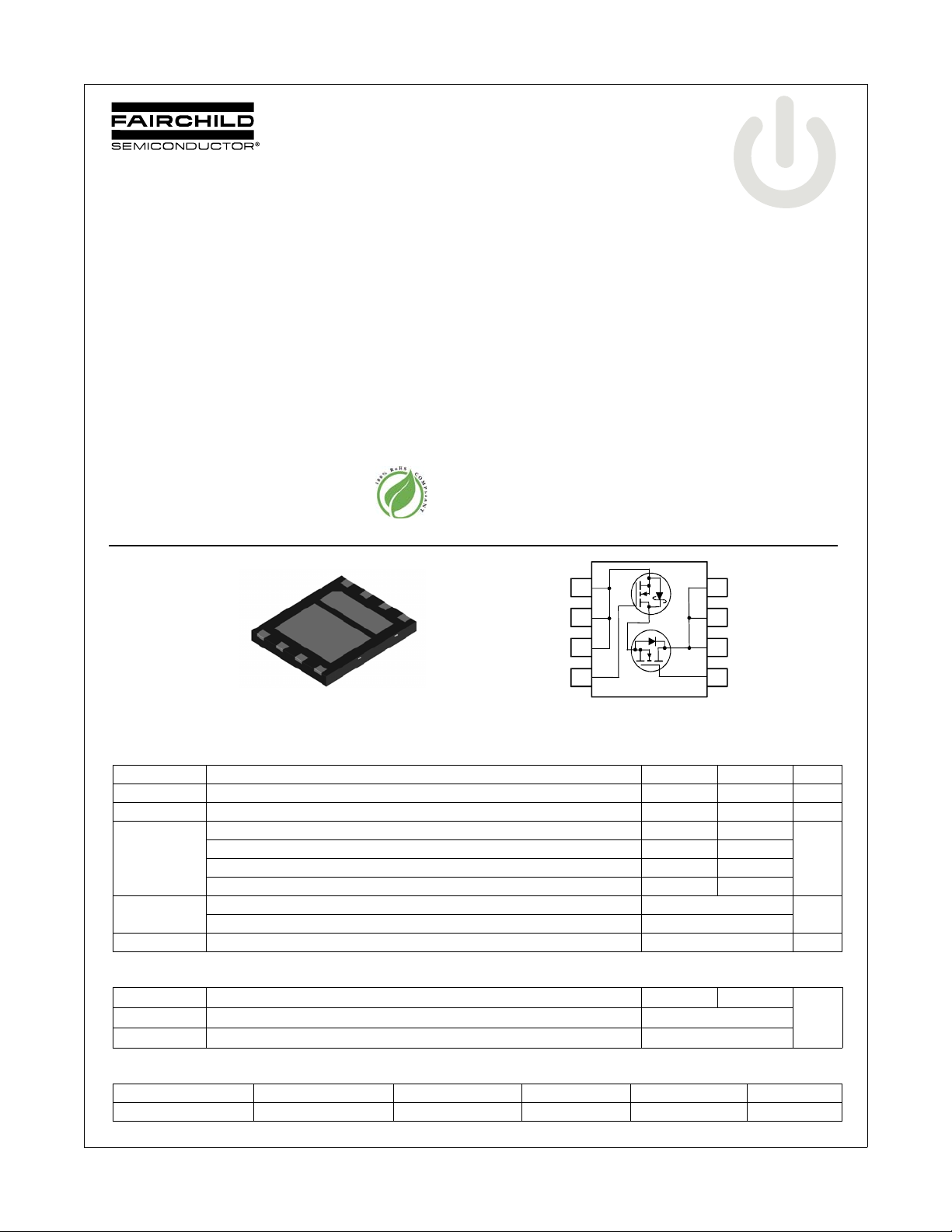
Dual N-Channel PowerTrench® MOSFET
Q1: 30V, 16A, 21.5mΩ Q2: 30V, 18A, 13mΩ
Features
Q1: N-Channel
Max r
Max r
Q2: N-Channel
Max r
Max r
Low Qg high side MOSFET
Low r
Thermally efficient dual Power 56 package
Pinout optimized for simple PCB design
RoHS Compliant
= 21.5mΩ at VGS = 10V, ID = 7.5A
DS(on)
= 29.5mΩ at VGS = 4.5V, ID = 6.5A
DS(on)
= 13mΩ at VGS = 10V, ID = 10A
DS(on)
= 17mΩ at VGS = 4.5V, ID = 8.5A
DS(on)
low side MOSFET
DS(on)
General Description
This device includes two specialized MOSFETs in a unique dual
Power 56 package. It is designed to provide an optimal
Synchronous Buck power stage in terms of efficiency and PCB
utilization. The low switching loss "High Side" MOSFET is
complemented by a Low Conduction Loss "Low Side" SyncFET .
Applications
Synchronous Buck Converter for:
Notebook System Power
General Purpose Point of Load
FDMS9620S Dual N-Channel PowerTrench
July 2007
®
MOSFET
MOSFET Maximum Ratings T
Symbol Parameter Q1 Q2 Units
V
DS
V
GS
I
D
P
D
, T
T
J
STG
Thermal Characteristics
R
θJC
θJA
R
θJA
Package Marking and Ordering Information
Device Marking Device Package Reel Size Tape Width Quantity
©2007 Fairchild Semiconductor Corporation
FDMS9620S Rev.D2
FDMS9620S FDMS9620S Power 56 13” 12mm 3000 units
Drain to Source Voltage 30 30 V
Gate to Source Voltage ±20 ±20 V
Drain Current -Continuous (Package limited) TC = 25°C 16 18
-Continuous (Silicon limited) T
-Continuous T
-Pulsed 60 60
Power Dissipation for Single Operation TA = 25°C (Note 1a) 2.5
T
Operating and Storage Junction Temperature Range -55 to +150 °C
Thermal Resistance, Junction to Case 8.2 3.1
Thermal Resistance, Junction to Ambient (Note 1a) 50
Thermal Resistance, Junction to Ambient (Note 1b) 120
= 25°C unless otherwise noted
A
= 25°C 21 44
C
= 25°C (Note 1a) 7.5 10
A
= 25°C (Note 1b) 1
A
1
A
W
°C/WR
www.fairchildsemi.com
FDMS9620S Dual N-Channel PowerTrench
Electrical Characteristics T
= 25°C unless otherwise noted
J
Symbol Parameter Test Conditions Type Min Typ Max Units
Off Characteristics
BV
ΔBV
ΔT
I
DSS
I
GSS
DSS
DSS
J
Drain to Source Breakdown Voltage
Breakdown Voltage Temperature
Coefficient
Zero Gate Voltage Drain Current VDS = 24V, V
ID = 250μA, VGS = 0V
ID = 1mA, VGS = 0V
ID = 250μA, referenced to 25°C
ID = 1mA, referenced to 25°C
= 0V
GS
Gate to Source Leakage Current VGS = ±20V, VDS= 0V
Q1Q230
30
Q1
Q2
Q1
Q2
Q1
Q2
V
23
23
mV/°C
1
500
±100
±100
On Characteristics
V
GS(th)
ΔV
ΔT
r
DS(on)
g
FS
GS(th)
J
Gate to Source Threshold Voltage
Gate to Source Threshold Voltage
Temperature Coefficient
Drain to Source On Resistance
Forward Transconductance
VGS = VDS, ID = 250μA
VGS = VDS, ID = 1mA
ID = 250μA, referenced to 25°C
ID = 1mA, referenced to 25°C
VGS = 10V, ID = 7.5A
VGS = 4.5V, ID = 6.5A
VGS = 10V , ID = 7.5A , TJ = 125°C
VGS = 10V, ID = 10A
VGS = 4.5V, ID = 8.5A
VGS = 10V, ID = 10A , TJ = 125°C
VDD = 10V, ID = 7.5A
VDD = 10V, ID = 10A
Q1Q21
Q1
Q2
Q1
Q2
Q1
Q2
1.6
1
1.6
-4
-4
18
23
25
9
13
14
3
3
mV/°C
21.5
29.5
32
13
17
22
25
27
μA
nA
V
mΩ
S
®
MOSFET
Dynamic Characteristics
C
iss
C
oss
C
rss
R
g
Input Capacitance
Output Capacitance
Reverse Transfer Capacitance
Gate Resistance f = 1MHz
Switching Characteristics
t
d(on)
t
r
t
d(off)
t
f
Q
g
Q
gs
Q
gd
Turn-On Delay Time
Rise Time
Turn-Off Delay Time
Fall Time
Total Gate Charge
Gate to Source Gate Charge
Gate to Drain “Miller” Charge
V
= 15V, VGS = 0V, f = 1MHZ
DS
VDD = 15V, ID = 1A,
V
= 10V, R
GS
GEN
= 6Ω
Q1
VDD = 15V, V
= 10V ,ID = 7.5A
GS
Q2
VDD = 15V, V
= 10V ,ID = 10A
GS
Q1
Q2
Q1
Q2
Q1
Q2
Q1
Q2
Q1
Q2
Q1
Q2
Q1
Q2
Q1
Q2
Q1
Q2
Q1
Q2
Q1
Q2
500
700
100
500
100
0.9
1.8
2.3
1.7
2.8
2.0
3.6
65
11
15
13
23
27
10
18
665
935
135
665
100
150
pF
pF
pF
Ω
20
27
7
14
24
37
44
10
7
14
14
25
ns
ns
ns
ns
nC
nC
nC
©2007 Fairchild Semiconductor Corporation
FDMS9620S Rev.D2
2
www.fairchildsemi.com
FDMS9620S Dual N-Channel PowerTrench
Electrical Characteristics T
= 25°C unless otherwise noted
J
Symbol Parameter Test Conditions Type Min Typ Max Units
Drain-Source Diode Characteristics
I
S
V
SD
t
rr
Q
rr
Notes:
1: R
is determined with the device mount ed on a 1 in2 pad 2 oz copper pad on a 1.5 x 1.5 in. board of FR-4 material. R
θJA
the user's board design.
Maximum Continuous Drain-Source Diode Forward Current
V
= 0V, IS = 2.1A (Note 2)
Source to Drain Diode Forward Voltage
Reverse Recovery Time
Reverse Recovery Charge
a.50°C/W when mounted on
a 1 in2 pad of 2 oz copper
GS
V
= 0V, IS = 3.5A (Note 2)Q1Q2
GS
Q1
I
= 7.5A, di/dt = 100A/μs
F
Q2
I
= 10A, di/dt = 300A/μs
F
Q1
Q2
0.7
0.5
Q1
Q2
Q1
Q2
is guaranteed by design while R
θJC
b. 120°C/W when mounted on a
minimum pad of 2 oz copper
13
14
2.1
3.5
1.2
1.0
4
9
is determined by
θCA
A
V
ns
nC
®
MOSFET
2: Pulse Test: Pulse Width < 300μs, Duty cycle < 2.0%.
©2007 Fairchild Semiconductor Corporation
FDMS9620S Rev.D2
3
www.fairchildsemi.com

FDMS9620S Dual N-Channel PowerTrench
01234
0
10
20
30
40
50
60
VGS = 4.5V
VGS = 4V
VGS = 3.5V
VGS = 10V
PULSE DURATION = 300μs
DUTY CYCLE = 2.0%MAX
VGS = 6V
I
D
, DRAIN CURRENT (A)
V
DS
, DRAIN TO SOURCE VOLTAGE (V)
0 102030405060
0.8
1.0
1.2
1.4
1.6
1.8
2.0
2.2
2.4
2.6
2.8
V
GS
= 10V
V
GS
= 6V
V
GS
= 4V
PULSE DURATION = 300μs
DUTY CYCLE = 2.0%MAX
NORMALIZED
DRAIN TO SOURCE ON-RESISTANCE
I
D
, DRAIN CURRENT(A)
V
GS
=3.5V
V
GS
= 4.5V
-50 -25 0 25 50 75 100 125 150
0.7
0.8
0.9
1.0
1.1
1.2
1.3
1.4
1.5
1.6
ID = 7.5A
V
GS
=10V
NORMALIZED
DRAIN TO SOURCE ON-RESISTANCE
TJ, JUNCTION TEMPERATURE (oC)
246810
10
20
30
40
50
60
70
PULSE DURATION = 300μs
DUTY CYCLE = 2.0%MAX
TJ = 125oC
T
J
= 25
o
C
ID = 3.8A
r
DS(on)
,
DRAIN TO
SOURCE ON-RESISTANCE
(mΩ)
V
GS
, GATE TO SOURCE VOL TA G E (V)
12345
0
10
20
30
40
VDD = 5V
PULSE DURATION = 300μs
DUTY CYCLE = 2.0%MAX
TJ =125oC
TJ = -55oC
TJ = 25oC
I
D
, DRAIN CURRENT (A)
V
GS
, GATE TO SOURCE VOLTAGE (V)
0.2 0.4 0.6 0.8 1.0 1.2 1.4
1E-3
0.01
0.1
1
10
TJ = -55oC
TJ = 25oC
TJ = 125oC
V
GS
= 0V
I
S
, REVERSE DRAIN CURRENT (A)
VSD, BODY DIODE FORWARD VOLTAGE (V)
60
Typical Characteristics (Q1 N-Channel)T
Figure 1. On Region Characteristics Figure 2. No rmali zed On -R esi st ance
= 25°C unless otherwise noted
J
vs Drain Current and Gate Voltage
®
MOSFET
Fi gu re 3. Normalized On Resistan c e
vs Junction Temperature
©2007 Fairchild Semiconductor Corporation
FDMS9620S Rev.D2
Figure 5. Transfer Characteristics Figure 6. Source to Drain Diode
Figure 4. On-Resistance vs Gate to
Source Voltage
Forward Voltage vs Source Current
4
www.fairchildsemi.com

FDMS9620S Dual N-Channel PowerTrench
024681012
0
2
4
6
8
10
ID = 7.5A
V
DD
= 20V
V
DD
= 15V
V
DD
=10V
Q
g
, GATE CHARGE(nC)
V
GS
, GATE TO SOURCE VOLTAGE(V)
0.1 1 10
100
1000
30
f = 1MHz
V
GS
= 0V
CAPACITANCE (pF)
VDS, DRAIN TO SOURCE VOLTAGE (V)
C
rss
C
oss
C
iss
30
0.1 1 10 100
0.01
0.1
1
10
100
DC
10s
1s
100ms
10ms
1ms
SINGLE PULSE
T
J
= MAX RATE
R
θJA
= 120
o
C
T
A
= 25
o
C
THIS AREA IS LIMITED
BY r
DS(ON)
VDS, DRAIN to SOURCE VOLTAGE (V)
I
D
, DRAIN CURRENT (A)
10-310
-2
10
-1
10010
1
10
2
10
3
1
10
100
0.5
VGS = 10V
SINGLE PULSE
R
θJA
= 120oC/W
T
A
= 25oC
P(
PK
), PEAK TRANSIENT POWER (W)
t, PULS E WIDTH (s)
10
-3
10
-2
10
-1
10
0
10
1
10
2
10
3
0.01
0.1
1
DUTY CYCLE-DESCENDING ORDER
NORMALIZED THERMAL
IMPEDANCE, Z
θJA
t, RECTANGULAR PULSE DURATION (s)
D = 0.5
0.2
0.1
0.05
0.02
0.01
SINGLE PULSE
R
θJA
= 120oC/W
2
P
DM
t
1
t
2
NOTES:
DUTY FACTOR: D = t1/t
2
PEAK TJ = PDM x Z
θJA
x R
θJA
+ T
A
Typical Characteristics (Q1 N-Channel)T
Figure 7. Gate Charge Characteristics Figure 8. Ca p ac i t an c e v s D ra i n
= 25°C unless otherwise noted
J
to Source Voltage
®
MOSFET
Figure 9. For w a rd B i a s Sa f e
Operating Area
©2007 Fairchild Semiconductor Corporation
FDMS9620S Rev.D2
Figure 10. Single Pulse Max imum
Figure 11. Transient Thermal Response Curve
5
Power Di ssipation
www.fairchildsemi.com

Typical Characteristics (Q2 SyncFET)
0.0 0.5 1.0 1.5 2.0 2.5
0
10
20
30
40
50
60
VGS = 4.5V
VGS = 4V
VGS = 3.5V
VGS = 10V
PULSE DURATION = 300μs
DUTY CYCLE = 2.0%MAX
VGS = 6V
I
D
, DRAIN CURRENT (A)
V
DS
, DRAIN TO SOURCE VOLTAGE (V)
0 102030405060
0.8
1.0
1.2
1.4
1.6
1.8
2.0
2.2
2.4
2.6
2.8
V
GS
= 10V
V
GS
= 6V
V
GS
= 4V
PULSE DURATION = 300μs
DUTY CYCLE = 2.0%MAX
NORMALIZED
DRAIN TO SOURCE ON-RESISTANCE
ID, DRAIN CURRENT(A)
V
GS
=3.5V
V
GS
= 4.5V
-50 -25 0 25 50 75 100 125 150
0.6
0.8
1.0
1.2
1.4
1.6
1.8
ID = 10A
V
GS
=10V
NORMALIZED
DRAIN TO SOURCE ON-RESISTANCE
T
J
, JUNCTION TE MPERATURE (
o
C)
246810
0
10
20
30
40
50
60
PULSE DURATION = 300μs
DUTY CYCLE = 2.0%MAX
TJ = 125oC
T
J
= 25
o
C
ID = 5A
r
DS(on)
, DRAIN TO
SOURCE ON-RESISTANCE (mΩ)
V
GS
, GATE TO SOURCE VOLTA G E (V)
12345
0
10
20
30
40
50
60
VDD = 5V
PULSE DURATION = 300μs
DUTY CYCLE = 2.0%MAX
TJ =125oC
TJ = -55oC
TJ = 25oC
I
D
, DRAIN CURRENT (A)
VGS, GATE TO SOURCE VOLTAGE (V)
0.0 0.2 0.4 0 .6 0.8
0.001
0.01
0.1
1
10
TJ = -55oC
TJ = 25oC
TJ = 125oC
V
GS
= 0V
I
S
, REVERSE DRAIN CURRENT (A)
VSD, BODY DIODE FORWARD VOLTAGE (V)
Figure 12. On-Region Characteristics Figure 13. Normalized on-Resistance vs Drain
FDMS9620S Dual N-Channel PowerTrench
Current and Gate Voltage
®
MOSFET
Figure 14. Normalized On-Resistance
vs Junction Temperature
©2007 Fairchild Semiconductor Corporation
FDMS9620S Rev.D2
Figure 16. Transfer Characteristics Figure 17. Source to Drain Diode
Figure 15. On-Resistance vs Gate to
Source Voltage
Forward Voltag e vs Source Current
6
www.fairchildsemi.com

Typical Characteristics
048121620
0
2
4
6
8
10
ID = 10A
V
DD
= 20V
V
DD
= 15V
V
DD
=10V
Q
g
, GATE CHARGE(nC)
V
GS
, GATE TO SOURCE VOLTAGE(V)
0.1 1 10
100
1000
2000
50
f = 1MHz
V
GS
= 0V
CAPACITANCE (pF)
VDS, DRAIN TO SOURCE VOLTAGE (V)
C
rss
C
oss
C
iss
30
FDMS9620S Dual N-Channel PowerTrench
Figure 18. Gate Charge Characteristics
Figure 19. Capacitance vs Drain
to Source Voltage
®
MOSFET
©2007 Fairchild Semiconductor Corporation
FDMS9620S Rev.D2
7
www.fairchildsemi.com

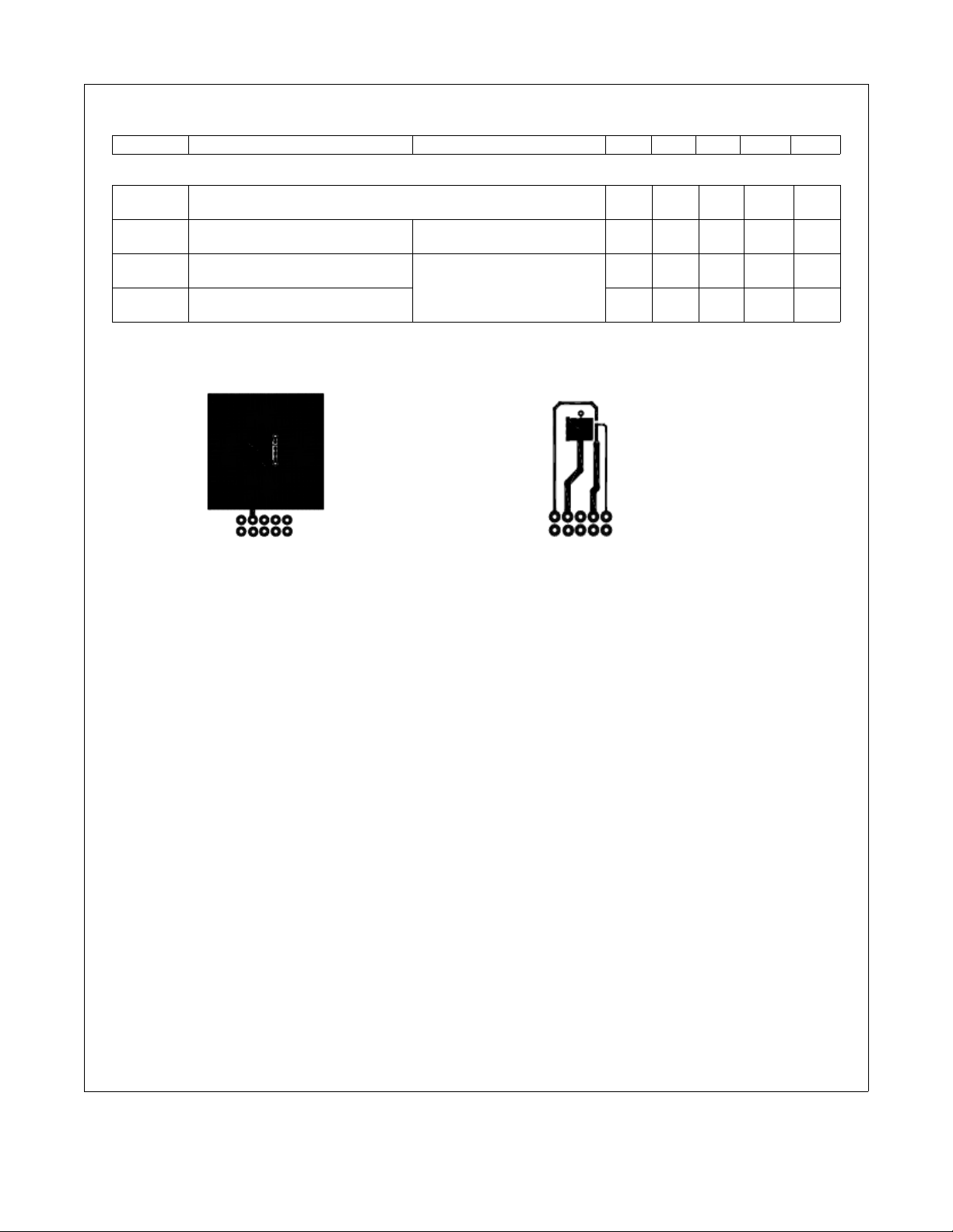
Dimensional Outline and Pad Layout
FDMS9620S Dual N-Channel PowerTrench
®
MOSFET
©2007 Fairchild Semiconductor Corporation
FDMS9620S Rev.D2
8
www.fairchildsemi.com

TRADEMARKS
The following are registered and unregistered trademarks and service marks Fairchild Semiconductor owns or is authorized to use and
is not intended to be an exhaustive list of all such trademarks.
®
ACEx
Build it Now™
CorePLUS™
CROSSVOLT™
CTL™
Current Transfer Logic™
EcoSPARK
Fairchild
®
®
Fairchild Semiconductor
FACT Quiet Series™
®
FACT
®
FAST
FastvCore™
FPS™
®
FRFET
Global Power Resource
®
SM
Green FPS™
Green FPS™ e-Series™
GTO™
i-Lo™
IntelliMAX™
ISOPLANAR™
MegaBuck™
MICROCOUPLER™
MicroFET™
MicroPak™
Motion-SPM™
OPTOLOGIC
OPTOPLANAR
®
PDP-SPM™
Power220
®
®
®
Power247
POWEREDGE
Power-SPM™
PowerTrench
Programmable Active Droop™
QFET
QS™
QT Optoelectronics™
Quiet Series™
RapidConfigure™
SMART START™
SPM
STEALTH™
SuperFET™
SuperSOT™-3
SuperSOT™-6
DISCLAIMER
FAIRCHILD SEMICONDUCTOR RESERVES THE RIGHT TO MAKE CHANGES WITHOUT FURTHER NOTICE TO ANY PRODUCTS
HEREIN TO IMPROVE RELIABILITY, FUNCTION, OR DESIGN. FAIRCHILD DOES NOT ASSUME ANY LIA BILITY ARISING OUT OF
THE APPLICATION OR USE OF ANY PRODUCT OR CIRCUIT DESCRIBED HEREIN; NEITHER DOES IT CO NVEY ANY LICENSE
UNDER ITS PATENT RIGHTS, NOR THE RIGHTS OF OTHERS. THESE SPECIFICATIONS DO NOT EXPAND THE TERMS OF
FAIRCHILD’S WORLDWIDE TERMS AND CONDITIONS, SPECIFICALLY THE WARRANTY THEREIN, WHICH COVERS THESE
PRODUCTS.
®
®
®
®
SuperSOT™-8
SyncFET™
The Power Franchise
TinyBoost™
TinyBuck™
TinyLogic
®
®
TINYOPTO™
TinyPower™
®
TinyPWM™
TinyWire™
µSerDes™
®
UHC
UniFET™
VCX™
LIFE SUPPORT POLICY
FAIRCHILD’S PRODUCTS ARE NOT AUTHORIZED FOR USE AS CRITICAL COMPONENTS IN LIFE SUPPORT DEVICES OR
SYSTEMS WITHOUT THE EXPRESS WRITTEN APPROVAL OF FAIRCHILD SEMICONDUCTOR CORPORATION.
As used herein:
1. Life support devices or systems are devices or systems
which, (a) are intended for surgical implant into the bo dy, or
(b) support or sustain life, and (c ) whose failure to perform
when properly used in accordance with instructions for use
2. A critical component is any component of a life support
device or system whose failure to perform can be reasonably
expected to cause the failure of the life support device or
system, or to affect its safety or effectiveness.
provided in the labeling, can be reasonably expected to result
in significant injury to the user.
PRODUCT STATUS DEFINITIONS
Definition of Terms
Datasheet Identification Product Status Definition
Advance Information Formative or In Design
This datasheet contains the design specifications for product development.
Specifications may change in any manner without notice.
This datasheet contains preliminary data; supplementary data will be pub-
Preliminary First Production
lished at a later date. Fairchild Semiconductor reserves the right to make
changes at any time without notice to improve design.
No Identification Needed Full Production
This datasheet contains final specifications. Fairchild Semiconductor reserves
the right to make changes at any time without notice to improve design.
This datasheet contains specifications on a product that has been discontin-
Obsolete Not In Production
ued by Fairchild semiconductor. The datasheet is printed for reference information only.
Rev. I30
 Loading...