

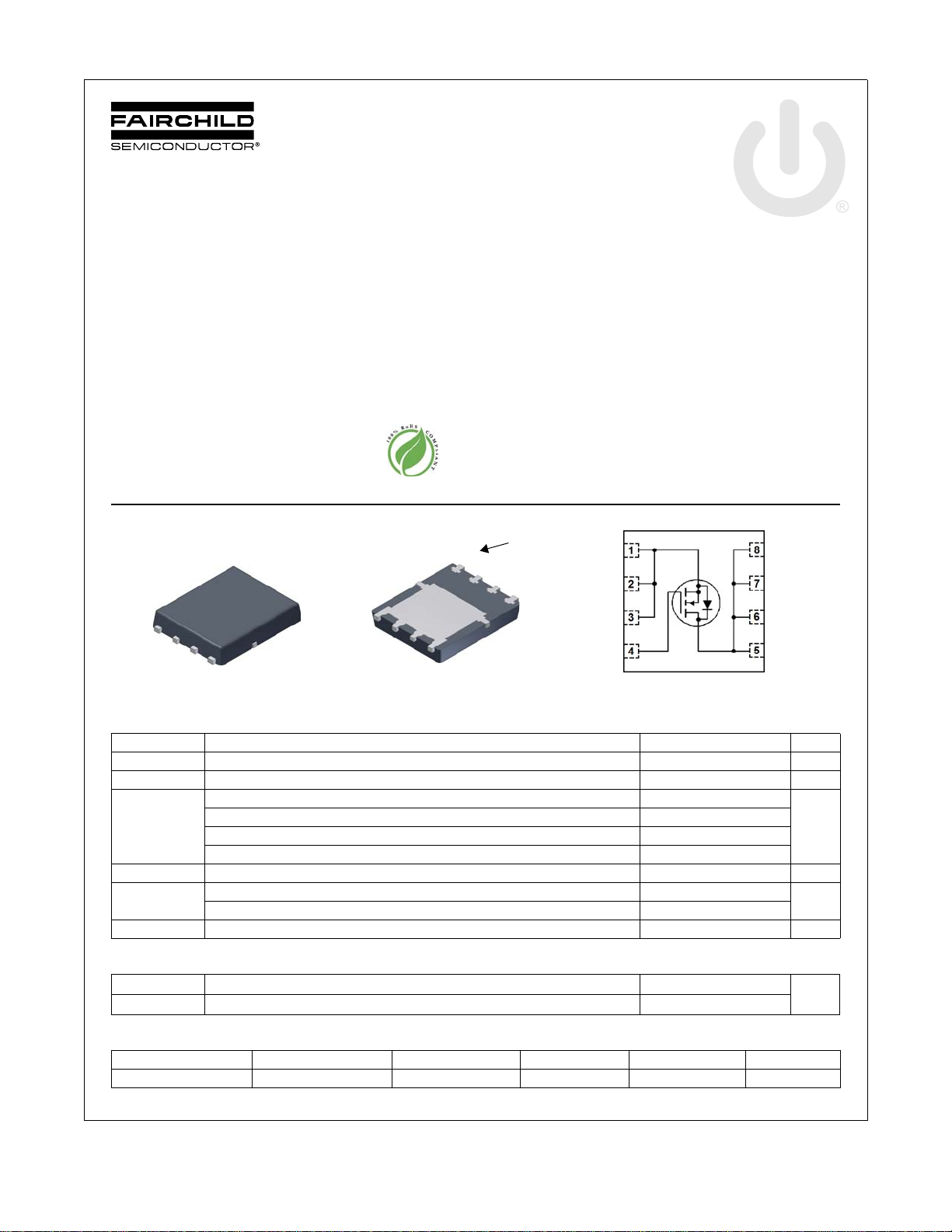
FDMS86540
Power 56
D
D
D
D
G
S
S
S
Pin 1
Bottom
Top
D
D
D
D
S
S
S
G
N-Channel PowerTrench® MOSFET
60 V, 50 A, 3.4 mΩ
Features
Max r
Max r
Advanced Package and Silicon combination for low r
and high efficiency
Next generation enhanced body diode technology,
engineered for soft recovery
MSL1 robust package design
100% UIL tested
RoHS Compliant
= 3.4 mΩ at VGS = 10 V, ID = 20 A
DS(on)
= 4.1 mΩ at VGS = 8 V, ID = 18.5 A
DS(on)
DS(on)
General Description
This N-Channel MOSFET has been designed specifically to
improve the overall efficiency and to minimize switch node
ringing of DC/DC converters using either synchronous or
conventional switching PWM controllers.It has been optimized
for low gate charge, low r
diode reverse recovery performance.
Applications
Primary Switch in isolated DC-DC
Synchronous Rectifier
Load Switch
December 2011
, fast switching speed and body
DS(on)
FDMS86540 N-Channel PowerTrench
®
MOSFET
MOSFET Maximum Ratings T
Symbol Parameter Ratings Units
V
DS
V
GS
I
D
E
AS
P
D
, T
T
J
STG
Drain to Source Voltage 60 V
Gate to Source Voltage ±20 V
Drain Current -Continuous (Package limited) TC = 25 °C 50
-Continuous (Silicon limited) T
-Continuous T
-Pulsed 120
Single Pulse Avalanche Energy (Note 3) 228 mJ
Power Dissipation TC = 25 °C 96
Power Dissipation T
Operating and Storage Junction Temperature Range -55 to +150 °C
= 25 °C unless otherwise noted
A
= 25 °C 126
C
= 25 °C (Note 1a) 20
A
= 25 °C (Note 1a) 2.5
A
A
W
Thermal Characteristics
R
θJC
R
θJA
Thermal Resistance, Junction to Case 1.3
Thermal Resistance, Junction to Ambient (Note 1a) 50
°C/W
Package Marking and Ordering Information
Device Marking Device Package Reel Size Tape Width Quantity
©2011 Fairchild Semiconductor Corporation
FDMS86540 Rev. C
FDMS86540 FDMS86540 Power 56 13 ’’ 12 mm 3000 units
1
www.fairchildsemi.com
FDMS86540 N-Channel PowerTrench
Electrical Characteristics T
= 25 °C unless otherwise noted
J
Symbol Parameter Test Conditions Min Typ Max Units
Off Characteristics
BV
ΔBV
ΔT
I
DSS
I
GSS
DSS
DSS
J
Drain to Source Breakdown Voltage ID = 250 μA, VGS = 0 V 60 V
Breakdown Voltage Temperature
Coefficient
Zero Gate Voltage Drain Current VDS = 48 V, V
Gate to Source Leakage Current VGS = ±20 V, V
I
= 250 μA, referenced to 25 °C 28 mV/°C
D
= 0 V 1 μA
GS
= 0 V ±100 nA
DS
On Characteristics
V
GS(th)
ΔV
ΔT
r
DS(on)
g
FS
GS(th)
J
Gate to Source Threshold Voltage VGS = VDS, ID = 250 μA23.24V
Gate to Source Threshold Voltage
Temperature Coefficient
Static Drain to Source On Resistance
I
= 250 μA, referenced to 25 °C -11 mV/°C
D
V
= 10 V, ID = 20 A 2.7 3.4
GS
= 8 V, ID = 18.5 A 3.1 4.1
GS
= 10 V, ID = 20 A, TJ = 125 °C 3.8 4.8
V
GS
Forward Transconductance VDS = 10 V, ID = 20 A 73 S
Dynamic Characteristics
C
iss
C
oss
C
rss
R
g
Input Capacitance
Output Capacitance 1413 1880 pF
Reverse Transfer Capacitance 50 90 pF
= 30 V, VGS = 0 V,
V
DS
f = 1 MHz
Gate Resistance 1.0 Ω
4837 6435 pF
Switching Characteristics
t
d(on)
t
r
t
d(off)
t
f
Q
Q
Q
Q
g
g
gs
gd
Turn-On Delay Time
Rise Time 16 29 ns
Turn-Off Delay Time 32 52 ns
= 30 V, ID = 20 A,
V
DD
V
= 10 V, R
GS
GEN
= 6 Ω
28 45 ns
Fall Time 7.2 15 ns
Total Gate Charge VGS = 0 V to 10 V
Total Gate Charge VGS = 0 V to 8 V 53 75 nC
Gate to Source Charge 23 nC
V
DD
I
= 20 A
D
= 30 V,
65 90 nC
Gate to Drain “Miller” Charge 12 nC
mΩV
®
MOSFET
Drain-Source Diode Characteristics
V
SD
t
rr
Q
rr
t
rr
Q
rr
Notes:
1. R
is determined with the device mounted on a 1 in2 pad 2 oz copper pad on a 1.5 x 1.5 in. boar d of FR-4 ma terial . R
θJA
the user's board design.
2. Pulse Test: Pulse Width < 300 μs, Duty cycle < 2.0%.
3. Starting TJ = 25 °C, L = 0.3 mH, IAS = 39 A, VDD = 54 V, VGS = 10 V.
©2011 Fairchild Semiconductor Corporation
FDMS86540 Rev. C
Source to Drain Diode Forward Voltage
Reverse Recovery Time
Reverse Recovery Charge 41 66 nC
Reverse Recovery Time
Reverse Recovery Charge 76 122 nC
a)
50 °C/W when mounted on a
1 in
SF
SS
DF
DS
G
2
pad of 2 oz copper
V
= 0 V, IS = 2.1 A (Note 2) 0.70 1.2
GS
= 0 V, IS = 20 A (Note 2) 0.79 1.3
V
GS
= 20 A, di/dt = 100 A/μs
I
F
= 20 A, di/dt = 300 A/μs
I
F
2
θJC
SF
SS
DF
DS
G
55 88 ns
44 70 ns
is guaranteed by design while R
125 °C/W when mounted on a
b)
minimum pad of 2 oz copper.
V
is determined by
θCA
www.fairchildsemi.com
FDMS86540 N-Channel PowerTrench
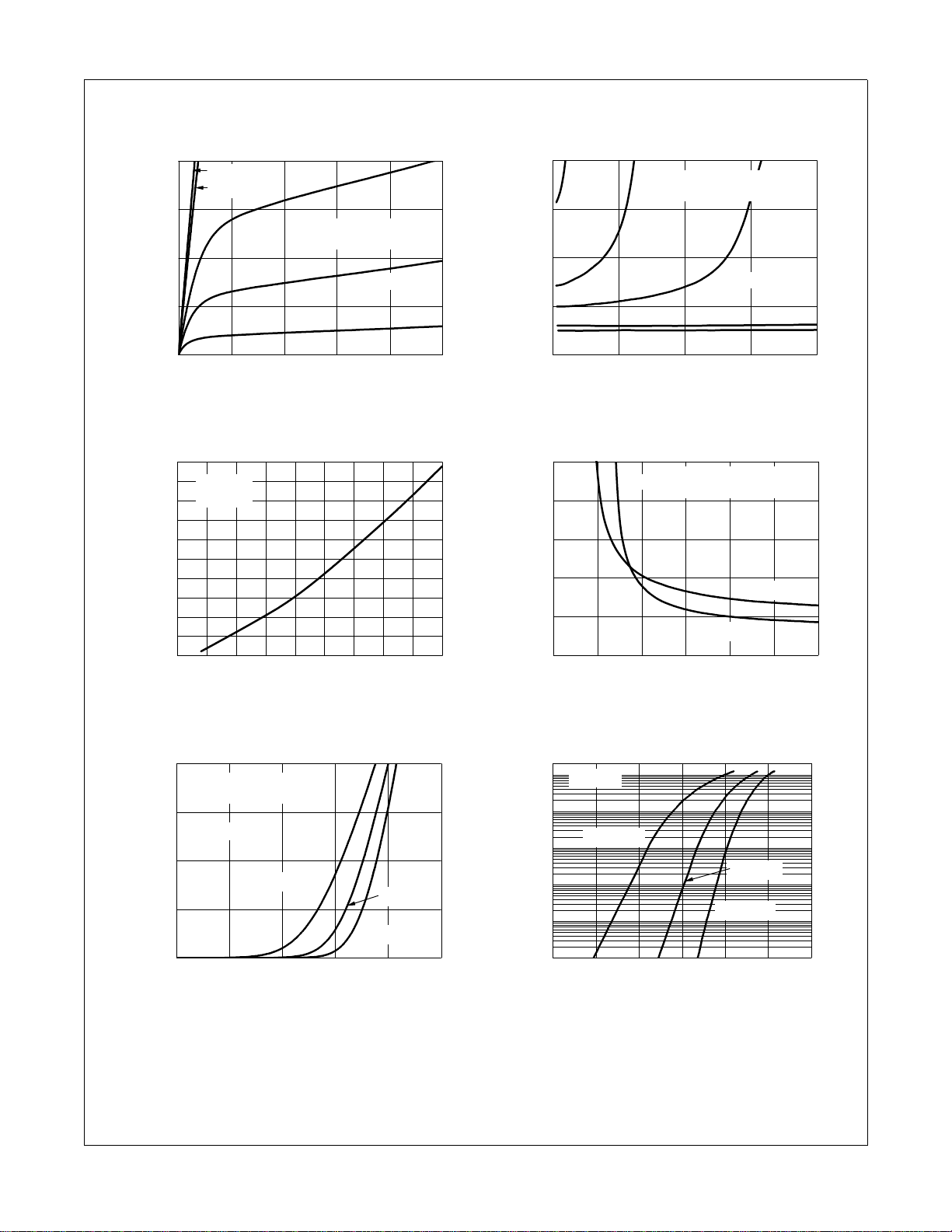
012345
0
30
60
90
120
VGS = 8 V
VGS = 6 V
VGS = 10 V
VGS = 5 V
VGS = 5.5 V
PULSE DURATION = 80 μs
DUTY CYCLE = 0.5% MAX
I
D
, DRAIN CURRENT (A)
VDS, DRAIN TO SOURCE VOLTAGE (V)
0 306090120
0
2
4
6
8
V
GS
= 8 V
PULSE DURATION = 80 μs
DUTY CYCLE = 0.5% MAX
NORMALIZED
DRAIN TO SOURCE ON-RESISTA NCE
I
D
, DRAIN CURRENT (A)
V
GS
= 6 V
VGS = 5.5 V
VGS = 5 V
V
GS
= 10 V
-75 -50 -25 0 25 50 75 100 125 150
0.7
0.8
0.9
1.0
1.1
1.2
1.3
1.4
1.5
1.6
1.7
ID = 20 A
V
GS
= 10 V
NORMALIZED
DRAIN TO SOURCE ON-RESISTANCE
T
J
, JUNCTION TE MPERATURE (
o
C)
45678910
0
3
6
9
12
15
TJ = 125 oC
ID = 20 A
TJ = 25 oC
V
GS
, GATE TO SOURCE VOLTA G E (V)
r
DS(on)
,
DRAIN TO
SOURCE ON-RESISTANCE
(mΩ)
PULSE DURATION = 80 μs
DUTY CYCLE = 0.5% MAX
234567
0
30
60
90
120
TJ = 25 oC
TJ = 150 oC
V
DS
= 5 V
PULSE DURATION = 80 μs
DUTY CYCLE = 0.5% MAX
TJ = -55 oC
I
D
, DRAIN CURRENT (A)
VGS, GATE TO SOURCE VOLTAGE (V)
0.0 0 .2 0.4 0.6 0.8 1.0 1.2
0.001
0.01
0.1
1
10
100
200
TJ = -55 oC
TJ = 25 oC
TJ = 150 oC
V
GS
= 0 V
I
S
, REVERSE DRAIN CURRENT (A)
VSD, BODY DIODE FORWARD VOLTAGE (V)
Typical Characteristics T
Figure 1.
On-Region Characteristics Figure 2.
= 25 °C unless otherwise noted
J
Nor ma liz ed O n-R esist anc e
vs Drain Current and Gate Voltage
®
MOSFET
Figur e 3 . No rm alize d On- R es ist an ce
vs Junction Temperature
©2011 Fairchild Semiconductor Corporation
FDMS86540 Rev. C
Figure 5. Transfer Characteristics
Figure 4.
On-Resistance vs Gate t o
Source Voltage
Figure 6.
Source to Drain Diode
Forward Voltage vs Source Current
3
www.fairchildsemi.com
 Loading...