FDMS86300
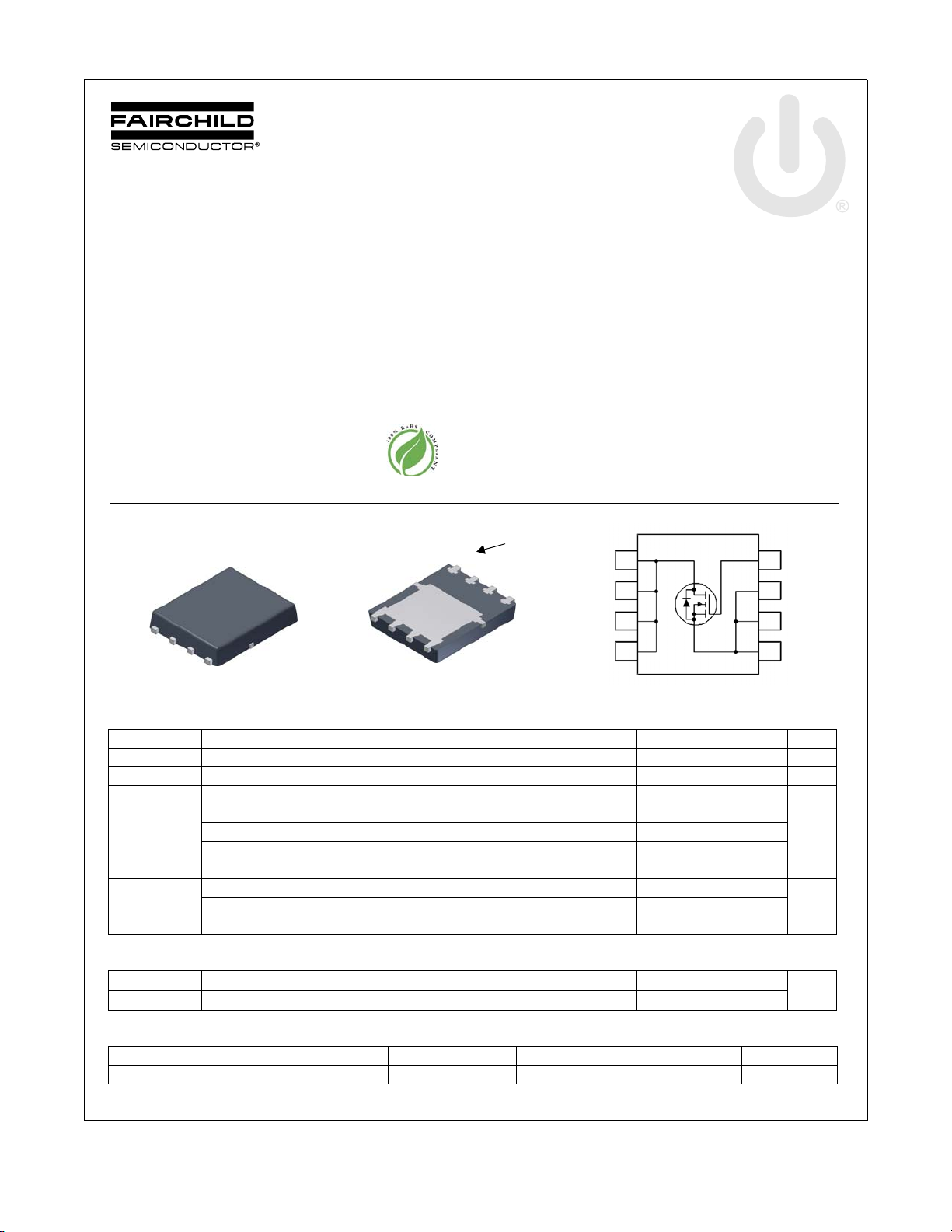
Power 56
D
D
D
D
G
S
S
S
Pin 1
Bottom
Top
G
S
S
S
D
D
D
D
5
6
7
8
3
2
1
4
N-Channel PowerTrench® MOSFET
80 V, 42 A, 3.9 mΩ
FDMS86300 N-Channel PowerTrench
August 2011
Features
Max r
Max r
Advanced Package and Silicon combination for low r
and high efficiency
Next generation enhanced body diode technology,
engineered for soft recovery
MSL1 robust package design
100% UIL tested
RoHS Compliant
= 3.9 mΩ at VGS = 10 V, ID = 19 A
DS(on)
= 5.5 mΩ at VGS = 8 V, ID = 15.5 A
DS(on)
DS(on)
General Description
This N-Channel MOSFET has been designed specifically to
improve the overall efficiency and to minimize switch node
ringing of DC/DC converters using either synchronous or
conventional switching PWM controllers.It has been optimized
for low gate charge, low r
diode reverse recovery performance.
, fast switching speed and body
DS(on)
Applications
OringFET / Load Switching
DC-DC Conversion
®
MOSFET
MOSFET Maximum Ratings T
Symbol Parameter Ratings Units
V
DS
V
GS
I
D
E
AS
P
D
, T
T
J
STG
Drain to Source Voltage 80 V
Gate to Source Voltage ±20 V
Drain Current -Continuous (Package limited) TC = 25 °C 42
-Continuous (Silicon limited) T
-Continuous T
-Pulsed 120
Single Pulse Avalanche Energy (Note 3) 252 mJ
Power Dissipation TC = 25 °C 104
Power Dissipation T
Operating and Storage Junction Temperature Range -55 to +150 °C
= 25 °C unless otherwise noted
A
= 25 °C 122
C
= 25 °C (Note 1a) 19
A
= 25 °C (Note 1a) 2.5
A
A
W
Thermal Characteristics
R
θJC
R
θJA
Thermal Resistance, Junction to Case 1.2
Thermal Resistance, Junction to Ambient (Note 1a) 50
°C/W
Package Marking and Ordering Information
Device Marking Device Package Reel Size Tape Width Quantity
©2011 Fairchild Semiconductor Corporation
FDMS86300 Rev.C
FDMS86300 FDMS86300 Power 56 13 ’’ 12 mm 3000 units
1
www.fairchildsemi.com

FDMS86300 N-Channel PowerTrench
Electrical Characteristics T
= 25 °C unless otherwise noted
J
Symbol Parameter Test Conditions Min Typ Max Units
Off Characteristics
BV
ΔBV
ΔT
I
DSS
I
GSS
DSS
DSS
J
Drain to Source Breakdown Voltage ID = 250 μA, VGS = 0 V 80 V
Breakdown Voltage Temperature
Coefficient
Zero Gate Voltage Drain Current VDS = 64 V, V
Gate to Source Leakage Current VGS = ±20 V, V
I
= 250 μA, referenced to 25 °C 39 mV/°C
D
= 0 V 1 μA
GS
= 0 V ±100 nA
DS
On Characteristics
V
GS(th)
ΔV
ΔT
r
DS(on)
g
FS
GS(th)
J
Gate to Source Threshold Voltage VGS = VDS, ID = 250 μA 2.5 3.4 4.5 V
Gate to Source Threshold Voltage
Temperature Coefficient
Static Drain to Source On Resistance
I
= 250 μA, referenced to 25 °C -11 mV/°C
D
V
= 10 V, ID = 19 A 3.2 3.9
GS
= 8 V, ID = 15.5 A 3.8 5.5
GS
= 10 V, ID = 19 A, TJ = 125 °C 5.0 5.8
V
GS
Forward Transconductance VDS = 10 V, ID = 19 A 60 S
Dynamic Characteristics
C
iss
C
oss
C
rss
R
g
Input Capacitance
Output Capacitance 957 1272 pF
Reverse Transfer Capacitance 26 63 pF
= 40 V, VGS = 0 V,
V
DS
f = 1 MHz
Gate Resistance 1.2 Ω
5325 7082 pF
Switching Characteristics
t
d(on)
t
r
t
d(off)
t
f
Q
Q
Q
Q
Turn-On Delay Time
Rise Time 26 43 ns
Turn-Off Delay Time 36 58 ns
= 40 V, ID = 19 A,
V
DD
V
= 10 V, R
GS
GEN
= 6 Ω
Fall Time 918ns
g
g
gs
gd
To tal Gate Charge VGS = 0 V to 10 V
To tal Gate Charge VGS = 0 V to 8 V 59 71 nC
Gate to Source Charge 28.2 nC
V
DD
I
= 19 A
D
= 40 V,
Gate to Drain “Miller” Charge 14.9 nC
31 50 ns
72 86 nC
mΩV
®
MOSFET
Drain-Source Diode Characteristics
V
V
SD
t
rr
Q
rr
t
rr
Q
rr
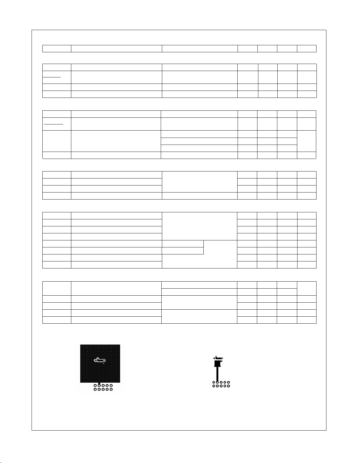
Notes:
1. R
is determined with the device mounted on a 1 in2 pad 2 oz copper pad on a 1.5 x 1.5 in. board of FR-4 material. R
θJA
the user's board design.
2. Pulse Test: Pulse Width < 300 μs, Duty cycle < 2.0%.
3. EAS of 252 mJ is based on starting TJ = 25 °C, L = 0.3 mH, IAS = 41 A, VDD = 72 V, VGS = 10 V.
©2011 Fairchild Semiconductor Corporation
FDMS86300 Rev.C
Source to Drain Diode Forward Voltage
Reverse Recovery Time
Reverse Recovery Charge 50 80 nC
Reverse Recovery Time
Reverse Recovery Charge 103 165 nC
a)
50 °C/W when mounted on a
2
1 in
pad of 2 oz copper
GS
V
GS
= 19 A, di/dt = 100 A/μs
I
F
= 19 A, di/dt = 300 A/μs
I
F
= 0 V, IS = 2.1 A (Note 2) 0.71 1.2
= 0 V, IS = 19 A (Note 2) 0.81 1.3
57 90 ns
48 77 ns
is guaranteed by design while R
θJC
b)
125 °C/W when mounted on a
minimum pad of 2 oz copper.
2
θCA
www.fairchildsemi.com
V
is determined by

FDMS86300 N-Channel PowerTrench
012345
0
30
60
90
120
VGS = 6.5 V
VGS = 10 V
VGS = 5.5 V
VGS = 6 V
VGS = 8 V
PULSE DURATION = 80 μs
DUTY CYCLE = 0.5% MAX
I
D
, DRAIN CURRENT (A)
VDS, DRA IN T O SOURCE VOLTAGE (V)
0306090120
0
1
2
3
4
5
VGS = 6.5 V
VGS = 5.5 V
PULSE DURA TION = 80 μs
DUTY CYCLE = 0.5% MAX
NORMALIZED
DRAIN TO SOURCE ON-RESISTANCE
I
D
, DRAIN CURRENT (A)
V
GS
= 8 V
VGS = 6 V
V
GS
= 10 V
-75 -50 -25 0 25 50 75 100 125 150
0.6
0.8
1.0
1.2
1.4
1.6
1.8
ID = 19 A
V
GS
= 10 V
NORMALIZED
DRAIN TO SOURCE ON-RESISTANCE
T
J
, JUNCTION TEMPERATURE (
o
C)
5678910
0
3
6
9
12
TJ = 125 oC
ID = 19 A
TJ = 25 oC
V
GS
, GATE TO SOURCE VOLTA G E (V)
r
DS(on)
,
DRAIN TO
SOURCE ON-RESISTANCE
(mΩ)
PULSE DURATION = 80 μs
DUTY CYCLE = 0.5% MAX
234567
0
30
60
90
120
TJ = 25 oC
TJ = 150 oC
V
DS
= 5 V
PULSE DURATION = 80 μs
DUTY CYCLE = 0.5% MAX
TJ = -55 oC
I
D
, DRAIN CURRENT (A)
VGS, GATE TO SOURCE VOLTAGE (V)
0.0 0 .2 0.4 0.6 0.8 1.0 1.2
0.001
0.01
0.1
1
10
100
200
TJ = -55 oC
TJ = 25 oC
TJ = 150 oC
V
GS
= 0 V
I
S
, REVERSE DRAIN CURRENT (A)
VSD, BODY DIODE FORWARD VOLTAGE (V)
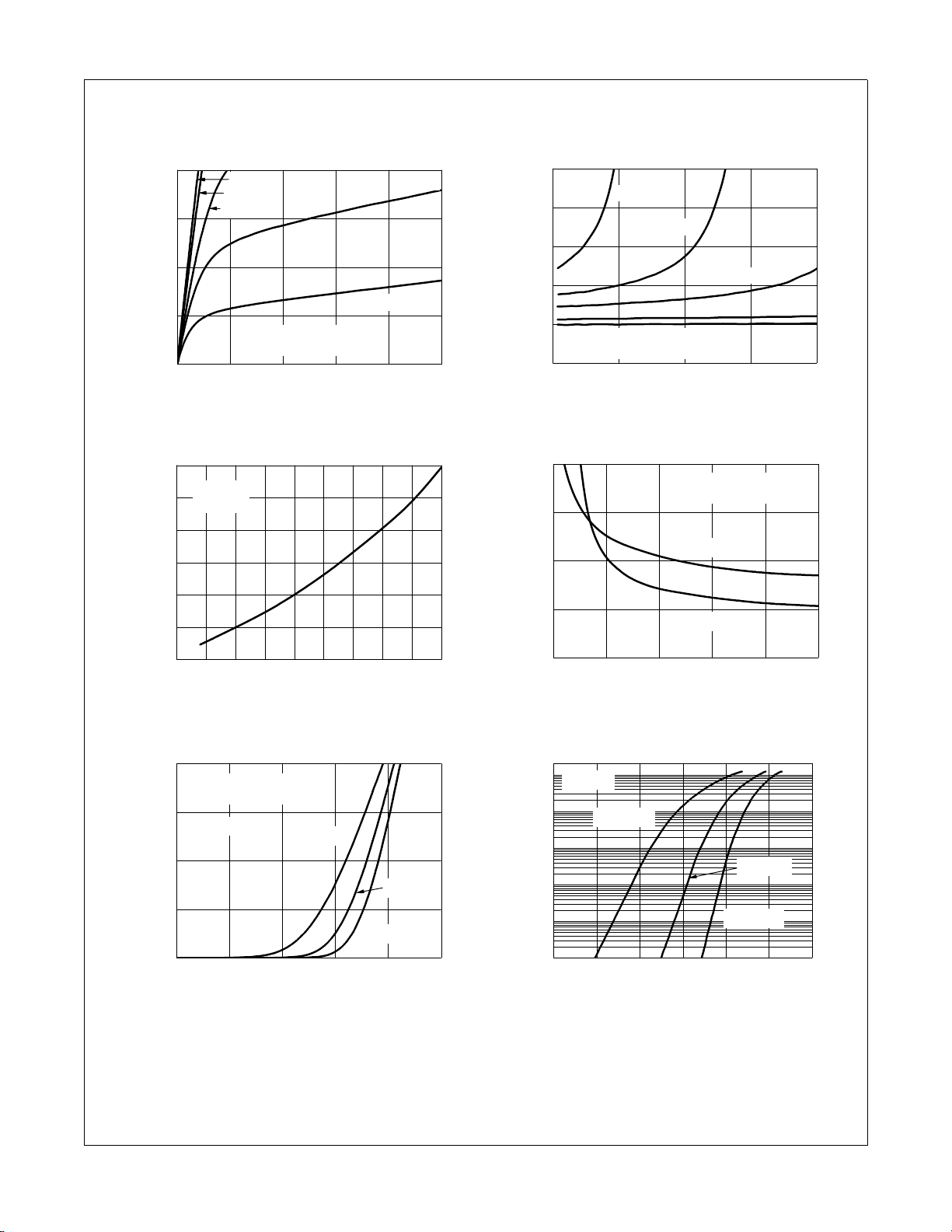
Typical Characteristics T
Figure 1.
On-Region Characteristics Figure 2.
= 25 °C unless otherwise noted
J
Norm a l i z e d O n -Resista n c e
vs Drain Current and Gate Voltage
®
MOSFET
Fig u r e 3. Nor m a lized O n - Resi s t ance
vs Junction Temperature
©2011 Fairchild Semiconductor Corporation
FDMS86300 Rev.C
Figure 5. Transfer Characteristics
Figure 4.
On-Resistance vs Ga te to
Source Voltage
Figure 6.
Source to Drain Diode
Forward Voltage vs Source Current
3
www.fairchildsemi.com
 Loading...