

Fairchild FDMS7692 service manual
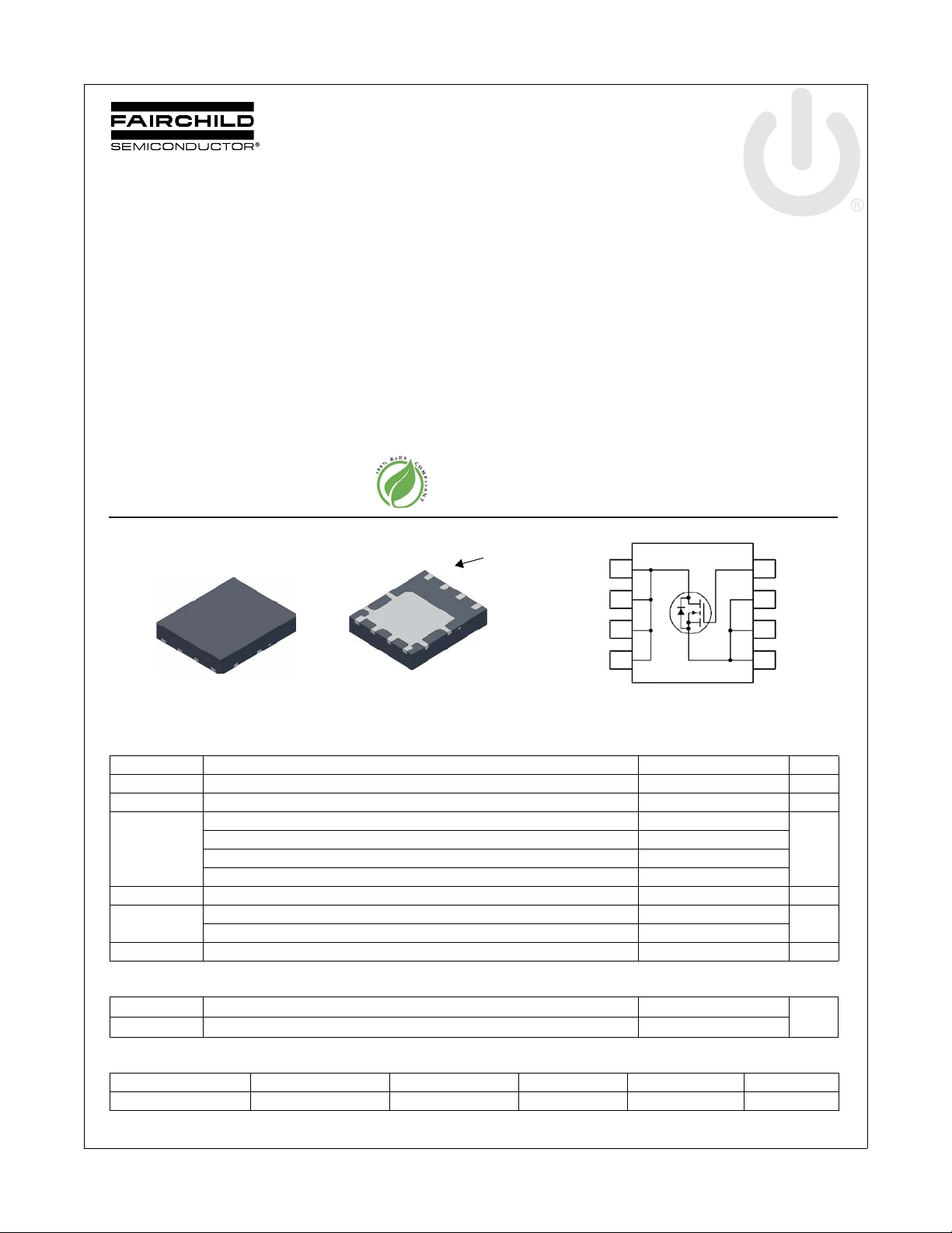
FDMS7692
G
S
S
S
D
D
D
D
5
6
7
8
3
2
1
4
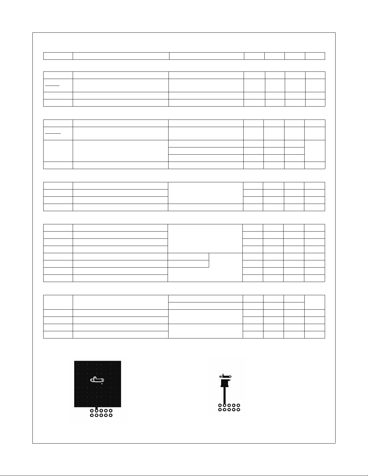
Bottom
Power 56
Top
Pin 1
G
S
S
S
D
D
D
D
N-Channel PowerTrench® MOSFET
30 V, 7.5 mΩ
FDMS7692 N-Channel PowerTrench
August 2011
Features
Max r
Max r
Advanced Package and Silicon combination for low r
and high efficiency
Next generation enhanced body diode technology, engineered
for soft recovery.
MSL1 robust package design
100% UIL tested
RoHS Compliant
= 7.5 mΩ at VGS = 10 V, ID = 13 A
DS(on)
= 13 mΩ at VGS = 4.5 V, ID = 10 A
DS(on)
DS(on)
General Description
This N-Channel MOSFET has been designed specifically to
improve the overall efficiency and to minimize switch node
ringing of DC/DC converters using either synchronous or
conventional switching PWM controllers. It has been optimized
for low gate charge, low r
diode reverse recovery performance.
fast switching speed and body
DS(on),
Applications
IMVP Vcore Switching for Notebook
VRM Vcore Switching for Desktop and Server
OringFET / Load Switch
DC-DC Conversion
®
MOSFET
MOSFET Maximum Ratings T
Symbol Parameter Ratings Units
V
DS
V
GS
I
D
E
AS
P
D
, T
T
J
STG
Drain to Source Voltage 30 V
Gate to Source Voltage ±20 V
Drain Current -Continuous (Package limited) TC = 25 °C 28
-Continuous (Silicon limited) T
-Continuous T
-Pulsed 50
Single Pulse Avalanche Energy (Note 3) 21 mJ
Power Dissipation TC = 25 °C 27
Power Dissipation T
Operating and Storage Junction Temperature Range -55 to +150 °C
= 25 °C unless otherwise noted
A
= 25 °C 47
C
= 25 °C (Note 1a) 14
A
= 25 °C (Note 1a) 2.5
A
A
W
Thermal Characteristics
R
θJC
R
θJA
Package Marking and Ordering Information
Device Marking Device Package Reel Size Tape Width Quantity
FDMS7692 FDMS7692 Power 56 13 ’’ 12 mm 3000 units
©2011 Fairchild Semiconductor Corporation
FDMS7692 Rev.D1
Thermal Resistance, Junction to Case 4.6
Thermal Resistance, Junction to Ambient (Note 1a) 50
1
°C/W
www.fairchildsemi.com
FDMS7692 N-Channel PowerTrench
Electrical Characteristics T
= 25 °C unless otherwise noted
J
Symbol Parameter Test Conditions Min Typ Max Units
Off Characteristics
BV
ΔBV
ΔT
I
DSS
I
GSS
DSS
DSS
J
Drain to Source Breakdown Voltage ID = 250 μA, VGS = 0 V 30 V
Breakdown Voltage Temperature
Coefficient
Zero Gate Voltage Drain Current VDS = 24 V, V
Gate to Source Leakage Current, Forward VGS = 20 V, V
I
= 250 μA, referenced to 25 °C 13 mV/°C
D
= 0 V 1 μA
GS
= 0 V 100 nA
DS
On Characteristics
V
GS(th)
ΔV
ΔT
r
DS(on)
g
FS
GS(th)
J
Gate to Source Threshold Voltage VGS = VDS, ID = 250 μA 1.2 2.0 3.0 V
Gate to Source Threshold Voltage
Temperature Coefficient
Static Drain to Source On Resistance
I
= 250 μA, referenced to 25 °C -6 mV/°C
D
V
= 10 V, ID = 13 A 6.5 7.5
GS
= 4.5 V, ID = 10 A 9.5 13
GS
= 10 V, ID = 13 A, TJ = 125 °C 9.0 1 1
V
GS
Forward Transconductance VDS = 5 V, ID = 13 A 68 S
Dynamic Characteristics
C
iss
C
oss
C
rss
R
g
Input Capacitance
Output Capacitance 325 435 pF
Reverse Transfer Capacitance 45 65 pF
Gate Resistance 1.0 2.0 Ω
Switching Characteristics
t
d(on)
t
r
t
d(off)
t
f
Q
Q
Q
Q
g
g
gs
gd
Turn-On Delay Time
Rise Time 2.7 10 ns
Turn-Off Delay Time 17 31 ns
Fall Time 2.3 10 ns
Total Gate Charge VGS = 0 V to 10 V
Total Gate Charge VGS = 0 V to 4.5 V 7 10 nC
Gate to Source Charge 3.4 nC
Gate to Drain “Miller” Charge 1.9 nC
= 15 V, VGS = 0 V,
V
DS
f = 1 MHz
= 15 V, ID = 13 A,
V
DD
V
= 10 V, R
GS
GEN
= 6 Ω
V
DD
I
= 13 A
D
= 15 V,
1015 1350 pF
816ns
15 22 nC
mΩV
®
MOSFET
Drain-Source Diode Characteristics
V
SD
t
rr
Q
rr
t
rr
Q
rr
Notes:
1. R
is determined with the device mounted on a 1 in2 pad 2 oz copper pad on a 1.5 x 1.5 in. board of FR- 4 mater ial. R
θJA
the user's board design.
2. Pulse Test: Pulse Width < 300 μs, Duty cycle < 2.0%.
3. Starting TJ = 25 °C, L = 0.3 mH, IAS = 12 A, VDD = 27 V, VGS = 10 V.
©2011 Fairchild Semiconductor Corporation
FDMS7692 Rev.D1
Source to Drain Diode Forward Voltage
Reverse Recovery Time
Reverse Recovery Charge 6 12 nC
Reverse Recovery Time
Reverse Recovery Charge 12 21 nC
a. 50 °C/W when mounted on a
2
1 in
pad of 2 oz copper.
V
= 0 V, IS = 2.1 A (Note 2) 0.75 1.1
GS
= 0 V, IS = 13 A (Note 2) 0.84 1.2
V
GS
= 13 A, di/dt = 100 A/μs
I
F
= 13 A, di/dt = 300 A/μs
I
F
2
θJC
21 34 ns
17 31 ns
is guaranteed by design while R
b. 125 °C/W when mounted on a
minimum pad of 2 oz copper.
V
is determined by
θCA
www.fairchildsemi.com
FDMS7692 N-Channel PowerTrench
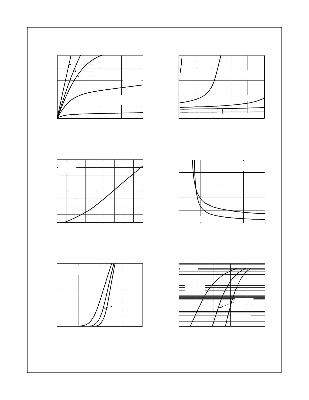
0.0 0.5 1.0 1.5 2.0
0
10
20
30
40
50
VGS = 3.5 V
VGS = 3.0 V
VGS = 4.0 V
PULSE DURATION = 80 μs
DUTY CYCLE = 0.5% MAX
VGS = 4.5 V
VGS = 10 V
I
D
, DRAIN CURRENT (A)
V
DS
, DRAIN TO SOURCE VOLTAGE (V)
0 1020304050
0
2
4
6
8
10
VGS = 3.5 V
NORMALIZED
DRAIN TO SOURCE ON-RESISTANCE
I
D
, DRAIN CURRENT (A)
V
GS
= 10 V
VGS = 4.0 V
VGS = 3.0 V
VGS = 4. 5 V
PULSE DURATION = 80 μs
DUTY CYCLE = 0.5% MAX
-75 -50 -25 0 25 50 75 100 125 150
0.8
0.9
1.0
1.1
1.2
1.3
1.4
1.5
1.6
ID = 13 A
V
GS
= 10 V
NORMALIZED
DRAIN TO SOURCE ON-RESISTANCE
T
J
, JUNCTION TEMPERATURE (
o
C)
246810
5
10
15
20
25
30
TJ = 125 oC
ID = 13 A
TJ = 25 oC
V
GS
, GATE TO S OURCE VOLTAGE (V)
r
DS(on)
,
DRAIN TO
SOURCE ON-RESISTANCE
(mΩ)
PULSE DURA TION = 80 μs
DUTY CYCLE = 0.5% MAX
12345
0
10
20
30
40
50
TJ = 150 oC
V
DS
= 5 V
PULSE DURATION = 80 μs
DUTY CYCLE = 0.5% MAX
TJ = -55 oC
TJ = 25 oC
I
D
, DRAIN CURRENT (A)
VGS, GATE TO SOURC E V OLTAGE (V)
0.2 0.4 0.6 0.8 1.0 1.2
0.01
0.1
1
10
100
TJ = -55 oC
TJ = 25 oC
TJ = 150 oC
V
GS
= 0 V
I
S
, REVERSE DRAIN CURRENT (A)
VSD, BODY DIODE FORWARD VOLTAGE (V)
Typical Characteristics T
Figure 1.
On Region Characteristics Figure 2.
= 25 °C unless otherwise noted
J
®
MOSFET
Nor ma liz ed O n-R esi st anc e
vs Drain Current and Gate Voltage
Fi gu re 3. Normalize d O n R es is ta nce
vs Junction Temperature
©2011 Fairchild Semiconductor Corporation
FDMS7692 Rev.D1
Figure 5. Transfer Characteristics
Figure 4.
On-Resistance vs Gate to
Source Voltage
Figure 6.
Sou rce to Drain Diode
Forward Voltage vs Source Current
3
www.fairchildsemi.com
 Loading...