Fairchild FDMS7620S service manual

FDMS7620S
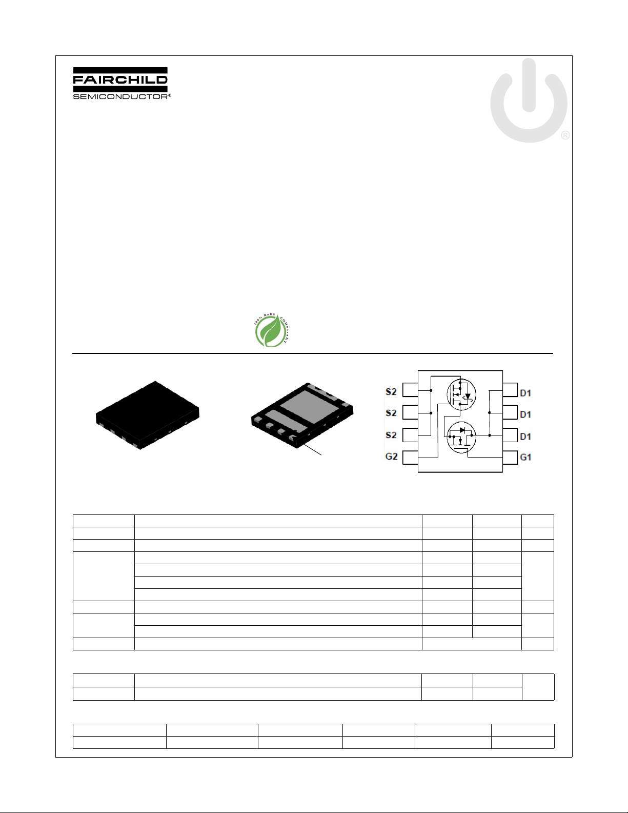
Power 56
S2
S2
S2
G2
D1
D1
D1
G1
D1
S1/D2
Top
Bottom
Pin1
4
Q 2
Dual N-Channel PowerTrench® MOSFET
Q1: 30 V, 10.1 A, 20.0 mΩ Q2: 30 V, 12.4 A, 11.2 mΩ
Features
Q1: N-Channel
Max r
Max r
Q2: N-Channel
Max r
Max r
Pinout optimized for simple PCB design
Thermally efficient dual Power 56 Package
RoHS Compliant
= 20.0 mΩ at VGS = 10 V, ID = 10.1 A
DS(on)
= 30.0 mΩ at VGS = 4.5 V, ID = 7.5 A
DS(on)
= 11.2 mΩ at VGS = 10 V, ID = 12.4 A
DS(on)
= 14.2 mΩ at VGS = 4.5 V, ID = 10.9 A
DS(on)
General Description
This device includes two specialized MOSFETs in a unique dual
Power 56 package. It is designed to provide an optimal synchro
nous buck power stage in terms of efficiency and PCB utilization.
The low switching loss “High Side” MOSFET is complementory
by a low conduction loss “Low Side” SyncFET.
Applications
Synchronous Buck Converter for:
Notebook System Power
General Purpose Point of Load
March 2011
FDMS7620S Dual N-Channel PowerTrench
-
®
MOSFET
5
6
7
8
MOSFET Maximum Ratings T
Symbol Parameter Q1 Q2 Units
V
DS
V
GS
I
D
E
AS
P
D
TJ, T
STG
Drain to Source Voltage 30 30 V
Gate to Source Voltage (Note 3) ±20 ±20 V
Drain Current -Continuous (Package limited) TC = 25 °C 13 22
-Continuous (Silicon limited) T
-Continuous T
-Pulsed 27 45
Single Pulse Avalanche Energy (Note 4) 9 21 mJ
Power Dissipation for Single Operation TA = 25°C 2.2
Power Dissipation for Single Operation T
Operating and Storage Junction Temperature Range -55 to +150 °C
= 25°C unless otherwise noted
A
= 25 °C 26 42
C
= 25 °C 10.1 12.4
A
= 25°C 1.0
A
3
2
1
Q 1
A
1a
1c
2.5
1.0
1b
1d
W
Thermal Characteristics
R
θJA
R
θJA
Package Marking and Ordering Information
©2011 Fairchild Semiconductor Corporation 1 www.fairchildsemi.com
FDMS7620S Rev.C1
Device Marking Device Package Reel Size Tape Width Quantity
FDMS7620S FDMS7620S Power 56 13 ” 12
Thermal Resistance, Junction to Ambient 57
Thermal Resistance, Junction to Ambient 125
1a
1c
mm 3000 units
50
120
1b
°C/W
1d

FDMS7620S Dual N-Channel PowerTrench
Electrical Characteristics T
= 25°C unless otherwise noted
J
Symbol Parameter Test Conditions Type Min Typ Max Units
Off Characteristics
BV
ΔBV
ΔT
I
DSS
I
GSS
DSS
DSS
J
Drain to Source Breakdown Voltage
Breakdown Voltage Temperature
Coefficient
Zero Gate Voltage Drain Current V
Gate to Source Leakage Current,
Forward
= 250 μA, VGS = 0 V
D
I
= 1 mA, VGS = 0 V
D
I
= 250 μA, referenced to 25°C
D
I
= 10 mA, referenced to 25°C
D
= 24 V, V
DS
V
= 20 V, V
GS
GS
DS
= 0 V
= 0 V
Q1Q230
30
Q1
Q2
Q1
Q2
Q1
Q2
V
19
19
mV/°C
1
500
100
100nAnA
I
On Characteristics
V
V
GS(th)
ΔV
ΔT
r
DS(on)
g
FS
GS(th)
J
Gate to Source Threshold Voltage
Gate to Source Threshold Voltage
Temperature Coefficient
Static Drain to Source On Resistance
Forward Transconductance
= VDS, I
GS
V
= VDS, I
GS
I
= 250 μA, referenced to 25°C
D
I
= 10 mA, referenced to 25°C
D
= 10 V, ID = 10.1 A
V
GS
V
= 4.5 V, ID = 7.5 A
GS
V
= 10 V, ID = 10 A, T
GS
V
= 10 V, ID = 12.4 A
GS
V
= 4.5 V, ID = 10.9 A
GS
V
= 10 V, ID = 12.4 A, T
GS
V
= 5 V, ID = 10.1 A
DD
V
= 5 V, ID = 12.4 A
DD
= 250 μA
D
= 1 mA
D
= 125°C
J
= 125°C
J
Q1Q21.0
1.0
Q1
Q2
Q1
Q2
Q1
Q2
2.2
2.0
-6
-5
15.2
22.7
18.7
8.3
10.5
8.9
22
53
3.0
3.0
mV/°C
20.0
30.0
22.5
11.2
14.2
15.1
μA
V
mΩ
S
®
MOSFET
Dynamic Characteristics
C
iss
C
oss
C
rss
R
g
Input Capacitance
Output Capacitance
Reverse Transfer Capacitance
Gate Resistance
Switching Characteristics
t
d(on)
t
r
t
d(off)
t
f
Q
g(TOT)
Q
g(TOT)
Q
gs
Q
gd
Turn-On Delay Time
Rise Time
Turn-Off Delay Time
Fall Time
Total Gate Charge V
Total Gate Charge V
Gate to Source Charge
Gate to Drain “Miller” Charge
457
= 15 V, VGS = 0 V, f = 1 MHZ
V
DS
Q1
Q2
Q1
Q2
Q1
Q2
Q1Q20.2
0.2
1050
167
358
22
35
1.6
1.2
608
1400
222
477
31
49
4.4
3.5
pF
pF
pF
Ω
Q1
V
= 15 V, ID = 10.1 A, R
DD
Q2
V
= 15 V, ID = 12.4 A, R
DD
= 0V to 10 V
GS
= 0V to 5 V
GS
Q1
V
= 15 V,
DD
I
= 10.1 A
D
Q2
V
= 15 V,
DD
I
= 12.4 A
D
GEN
GEN
= 6 Ω
= 6 Ω
Q1
Q2
Q1
Q2
Q1
Q2
Q1
Q2
Q1
Q2
Q1
Q2
Q1
Q2
Q1
Q2
5.2
6.61014
1.2
1.81010
11.9
17.42232
1.4
1.51010
7.2
15.61123
3.8
7.9612
1.6
3.2
1.1
1.6
ns
ns
ns
ns
nC
nC
nC
nC
©2011 Fairchild Semiconductor Corporation 2 www.fairchildsemi.com
FDMS7620S Rev.C1

Electrical Characteristics T
= 25°C unless otherwise noted
J
Symbol Parameter Test Conditions Type Min Typ Max Units
Drain-Source Diode Characteristics
V
= 0 V, IS = 10.1 A (Note 2)
V
SD
t
rr
Q
rr
Notes:
1. R
is determined with the device mounted on a 1 in2 pad 2 oz copper pad on a 1.5 x 1.5 in. board of FR-4 material. R
θJA
by the user's board design.
Source-Drain Diode Forward Voltage
Reverse Recovery Time
Reverse Recovery Charge
GS
V
= 0 V, IS = 12.4 A (Note 2)
GS
Q1
I
= 10.1 A, di/dt = 100 A/s
F
Q2
I
= 12.4 A, di/dt = 300 A/s
F
Q1
Q2
0.90
0.83
Q1
Q2
Q1
Q2
is guaranteed by design while R
θJC
16
18
13
1.2
1.2
28
32
4
10
23
is determined
θCA
FDMS7620S Dual N-Channel PowerTrench
V
ns
nC
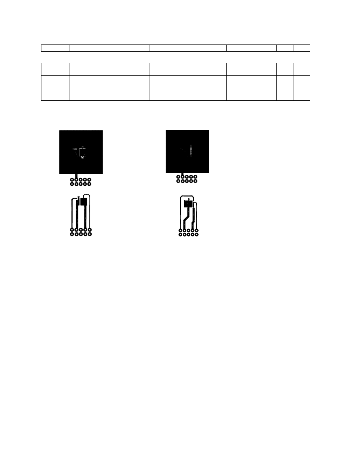
a. 57 °C/W when mounted on
a 1 in2 pad of 2 oz copper
c. 125 °C/W when mounted on a
minimum pad of 2 oz copper
2. Pulse Test: Pulse Width < 300 μs, Duty cycle < 2.0%.
3. As an N-ch device, the negative Vgs rating is for low duty cycle pulse ocurrence only. No continuous rating is implied.
4. Q1: E
of 9 mJ is based on starting TJ = 25 oC, L = 0.3 mH, IAS = 8 A, VDD = 27 V, VGS = 10 V. 100% test at L = 3 mH, IAS = 2.0 A, VDD = 0 V, VGS = 15 V.
AS
Q2: E
of 21 mJ is based on starting TJ = 25 oC, L = 0.3 mH, IAS = 12 A, VDD = 27 V, VGS = 10 V. 100% test at L = 3 mH, IAS = 3.2A, VDD = 0 V,VGS = 15 V..
AS
b. 50 °C/W when mounted on
2
a 1 in
pad of 2 oz copper
d. 120 °C/W when mounted on a
minimum pad of 2 oz copper
®
MOSFET
©2011 Fairchild Semiconductor Corporation 3 www.fairchildsemi.com
FDMS7620S Rev.C1

FDMS7620S Dual N-Channel PowerTrench
0.0 0.5 1.0 1.5 2.0 2.5 3.0
0
3
6
9
12
15
18
21
24
27
V
GS
= 6 V
V
GS
= 4 V
V
GS
= 10 V
V
GS
= 4.5 V
V
GS
= 3.5 V
PULSE DURATION = 80 μs
DUTY CYCLE = 0.5% MAX
I
D
, DRAIN CURRENT (A)
V
DS
, DRAIN TO SOURCE VOLTAGE (V)
0 3 6 9 12 15 18 21 24 27
0
1
2
3
4
5
6
VGS = 6 V
VGS = 3.5 V
PULSE DURATION = 80 μs
DUTY CYCLE = 0.5% MAX
NORMALIZED
DRAIN TO SOURCE ON-RESISTA NCE
I
D
, DRAIN CURRENT (A)
V
GS
= 4 V
VGS = 4.5 V
V
GS
= 10 V
-75 -50 -25 0 25 50 75 100 125 150
0.6
0.8
1.0
1.2
1.4
1.6
ID = 10.1 A
V
GS
= 10 V
NORMALIZED
DRAIN TO SOURCE ON-RESISTANC E
T
J
, JUNCTION TEMPERATUR E (
o
C)
345678910
0
10
20
30
40
50
60
TJ = 125 oC
ID = 10.1 A
TJ = 25 oC
V
GS
, GATE TO SOURCE VOLTAGE (V)
r
DS(on)
,
DRAIN TO
SOURCE ON-RESISTANCE
(mΩ)
PULSE DURATION = 80 μs
DUTY CYCLE = 0.5% MAX
1.5 2.0 2.5 3.0 3.5 4.0 4.5 5.0
0
3
6
9
12
15
18
21
24
27
TJ = 150 oC
V
DS
= 5 V
PULSE DURATION = 80 μs
DUTY CYCLE = 0.5% MAX
TJ = -55 oC
TJ = 25 oC
I
D
, DRAIN CURRENT (A)
VGS, GATE TO SOURCE VOLTAGE (V)
0.0 0.2 0.4 0.6 0.8 1.0 1.2
0.001
0.01
0.1
1
10
30
TJ = -55 oC
TJ = 25 oC
TJ = 150 oC
V
GS
= 0 V
I
S
, REVERSE DRAIN CURRENT (A)
VSD, BODY DIODE FORWARD VOLTAGE (V)
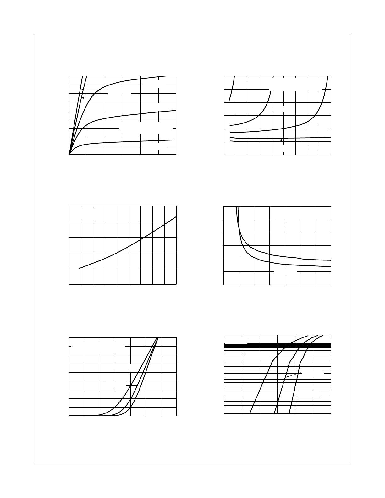
Typical Characteristics (Q1 N-Channel) T
Figure 1.
On Region Characteristics Figure 2.
= 25°C unless otherwise noted
J
Normali z e d O n - R esistance
vs Drain Current and Gate Voltage
®
MOSFET
Fig u re 3. Norma lized O n Res i stan c e
vs Junction Temperature
©2011 Fairchild Semiconductor Corporation 4 www.fairchildsemi.com
FDMS7620S Rev.C1
Figure 5. Transfer Characteristics
Figure 4.
On-R esistance vs Gate to
Source Voltage
Figure 6.
Source to Drain Diode
Forward Voltage vs Source Current
 Loading...