


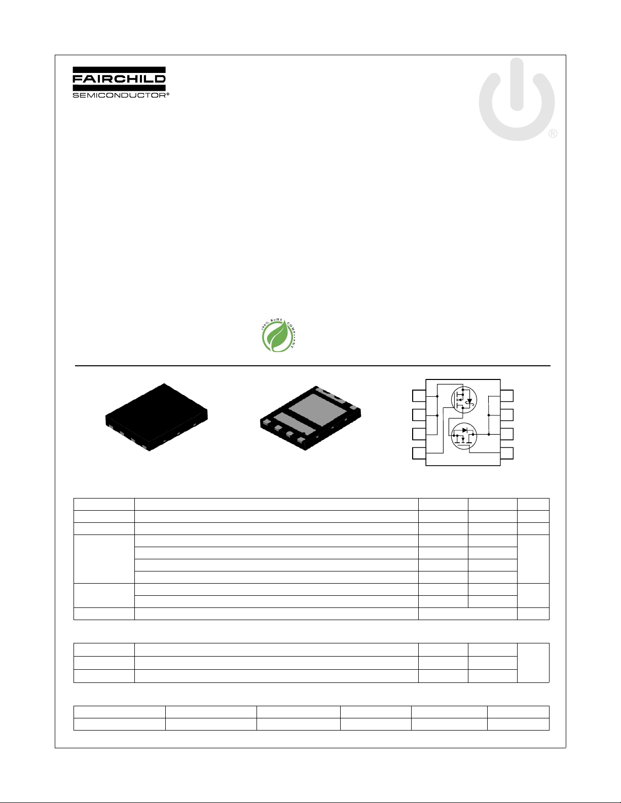
FDMS7600AS
Dual N-Channel PowerTrench® MOSFET
N-Channel: 30 V, 30 A, 7.5 mΩ N-Channel: 30 V, 40 A, 2.8 mΩ
Features
Q1: N-Channel
Max r
Max r
Q2: N-Channel
Max r
Max r
RoHS Compliant
= 7.5 mΩ at VGS = 10 V, ID = 12 A
DS(on)
= 12 mΩ at VGS = 4.5 V, ID = 10 A
DS(on)
= 2.8 mΩ at VGS = 10 V, ID = 20 A
DS(on)
= 3.3 mΩ at VGS = 4.5 V, ID = 18 A
DS(on)
General Description
This device includes two specialized N-Channel MOSFETs in a
dual MLP package.The switch node has been internally
connected to enable easy placement and routing of synchronous
buck converters. The control MOSFET (Q1) and synchronous
SyncFET (Q2) have been designed to provide optimal power
efficiency.
Applications
Computing
FDMS7600AS Dual N-Channel PowerTrench
December 2009
Communications
General Purpose Point of Load
Notebook V
S2
S2
S1/D2
D1
D1
D1
D1
Top
MOSFET Maximum Ratings T
Symbol Parameter Q1 Q2 Units
V
DS
V
GS
I
D
P
D
TJ, T
STG
Drain to Source Voltage 30 30 V
Gate to Source Voltage (Note 3) ±20 ±20 V
Drain Current -Continuous (Package limited) TC = 25 °C 30 40
-Continuous (Silicon limited) T
-Continuous T
-Pulsed 40 60
Power Dissipation for Single Operation TA = 25 °C 2.2
T
Operating and Storage Junction Temperature Range -55 to +150 °C
Power 56
= 25 °C unless otherwise noted
A
G1
Bottom
S2
G2
CORE
S2
S2
S2
G2
= 25 °C 50 120
C
= 25 °C 12
A
= 25 °C 1.0
A
Q 2
5
6
7
8
1a
1a
1c
Q 1
1b
22
1b
2.5
1d
1.0
Thermal Characteristics
R
θJA
θJA
R
θJC
Thermal Resistance, Junction to Ambient 57
Thermal Resistance, Junction to Ambient 125
Thermal Resistance, Junction to Case 3.5 2
1a
1c
50
120
1b
1d
Package Marking and Ordering Information
®
MOSFET
D1
4
D1
3
D1
2
G1
1
A
W
°C/WR
Device Marking Device Package Reel Size Tape Width Quantity
FDMS7600AS FDMS7600AS Power 56 13 ” 12 mm 3000 units
©2009 Fairchild Semiconductor Corporation
FDMS7600AS Rev.C
1
www.fairchildsemi.com
FDMS7600AS Dual N-Channel PowerTrench
Electrical Characteristics T
= 25 °C unless otherwise noted
J
Symbol Parameter Test Conditions Type Min Typ Max Units
Off Characteristics
BV
∆BV
∆T
I
DSS
I
GSS
DSS
DSS
J
Drain to Source Breakdown Voltage
Breakdown Voltage Temperature
Coefficient
Zero Gate Voltage Drain Current VDS = 24 V, V
Gate to Source Leakage Current VGS = 20 V, VDS= 0 V
On Characteristics
V
GS(th)
∆V
∆T
r
DS(on)
g
FS
GS(th)
J
Gate to Source Threshold Voltage
Gate to Source Threshold Voltage
Temperature Coefficient
Drain to Source On Resistance
Forward Transconductance
ID = 250 µA, VGS = 0 V
ID = 1 mA, VGS = 0 V
ID = 250 µA, referenced to 25 °C
ID = 1 mA, referenced to 25 °C
= 0 V
GS
VGS = VDS, ID = 250 µA
VGS = VDS, ID = 1 mA
ID = 250 µA, referenced to 25 °C
ID = 1 mA, referenced to 25 °C
VGS = 10 V, ID = 12 A
VGS = 4.5 V, ID = 10 A
VGS = 10 V , ID = 12 A , TJ = 125 °C
VGS = 10 V, ID = 20 A
VGS = 4.5 V, ID = 18 A
VGS = 10 V , ID = 20 A , TJ = 125 °C
VDS = 5 V, ID = 12 A
VDS = 5 V, ID = 20 A
Q1Q230
30
Q1
Q2
Q1
Q2
Q1
Q2
Q1Q21
Q1
Q2
Q1
Q2
Q1
Q2
1
15
18
1.8
1.5
6.0
8.5
8.3
2.2
2.6
2.6
63
190
V
mV/°C
1
500µAµA
100
100nAnA
3
3
-6
-5
mV/°C
7.5
12
12
2.8
3.3
3.8
V
mΩ
S
®
MOSFET
Dynamic Characteristics
C
iss
C
oss
C
rss
R
g
Input Capacitance
Output Capacitance
Reverse Transfer Capacitance
Gate Resistance
Switching Characteristics
t
d(on)
t
r
t
d(off)
t
f
Q
g
Q
g
Q
gs
Q
gd
Turn-On Delay Time
Rise Time
Turn-Off Delay Time
Fall Time
Total Gate Charge V
Total Gate Charge V
Gate to Source Gate Charge
Gate to Drain “Miller” Charge
Q1:
V
= 15 V, VGS = 0 V, f = 1 MHZ
DS
Q2:
V
= 15 V, VGS = 0 V, f = 1 MHZ
DS
Q1:
VDD = 15 V, ID = 12 A,
VGS = 10 V, R
GEN
= 6 Ω
Q2:
VDD = 15 V, ID = 20 A,
VGS = 10 V, R
= 0 V to 10 V
GS
GEN
= 6 Ω
Q1
VDD = 15 V,
= 0 V to 4.5 V
GS
ID = 12 A
Q2
VDD = 15 V,
ID = 20 A
Q1
Q2
Q1
Q2
Q1
Q2
Q1
Q2
Q1
Q2
Q1
Q2
Q1
Q2
Q1
Q2
Q1
Q2
Q1
Q2
Q1
Q2
Q1
Q2
1315
1750
5265
7005
445
2150
600
2860
45
20070300
0.9
0.3
8.61818
2.5
7.61016
20
45
2.3
5.21010
20
8128113
9.33713
4.3
13
2.2
9.6
32
32
72
52
pF
pF
pF
Ω
ns
ns
ns
ns
nC
nC
nC
nC
©2009 Fairchild Semiconductor Corporation
FDMS7600AS Rev.C
2
www.fairchildsemi.com
FDMS7600AS Dual N-Channel PowerTrench
Electrical Characteristics T
= 25 °C unless otherwise noted
J
Symbol Parameter Test Conditions Type Min Typ Max Units
Drain-Source Diode Characteristics
0.8
V
= 0 V, IS = 12 A (Note 2)
V
SD
t
rr
Q
rr
Notes:
1: R
is determined with the device mounted on a 1 in2 pad 2 oz copper pad o n a 1. 5 x 1.5 in. board of FR-4 material. R
θJA
by the user's board design.
Source to Drain Diode Forward Voltage
Reverse Recovery Time
Reverse Recovery Charge
a. 57 °C/W when mounted on
2
a 1 in
pad of 2 oz copper
c. 125 °C/W when mounted on a
minimum pad of 2 oz copper
GS
V
= 0 V, IS = 20 A (Note 2)Q1Q2
GS
Q1
I
= 12 A, di/dt = 100 A/µs
F
Q2
I
= 20 A, di/dt = 300 A/µs
F
Q1
Q2
Q1
Q2
is guaranteed by design while R
θJC
b. 50 °C/W when mounted on
a 1 in
d. 120 °C/W when mounted on a
minimum pad of 2 oz copper
2
pad of 2 oz copper
0.7
274743
108018
128
1.2
1.2
75
is determined
θCA
V
ns
nC
®
MOSFET
2: Pulse Test: Pulse Width < 300 µs, Duty cycle < 2.0%.
3: As an N-ch device, the negative Vgs rating is for low duty cycle pulse ocurrence only. No continuous rating is implied.
©2009 Fairchild Semiconductor Corporation
FDMS7600AS Rev.C
3
www.fairchildsemi.com
FDMS7600AS Dual N-Channel PowerTrench
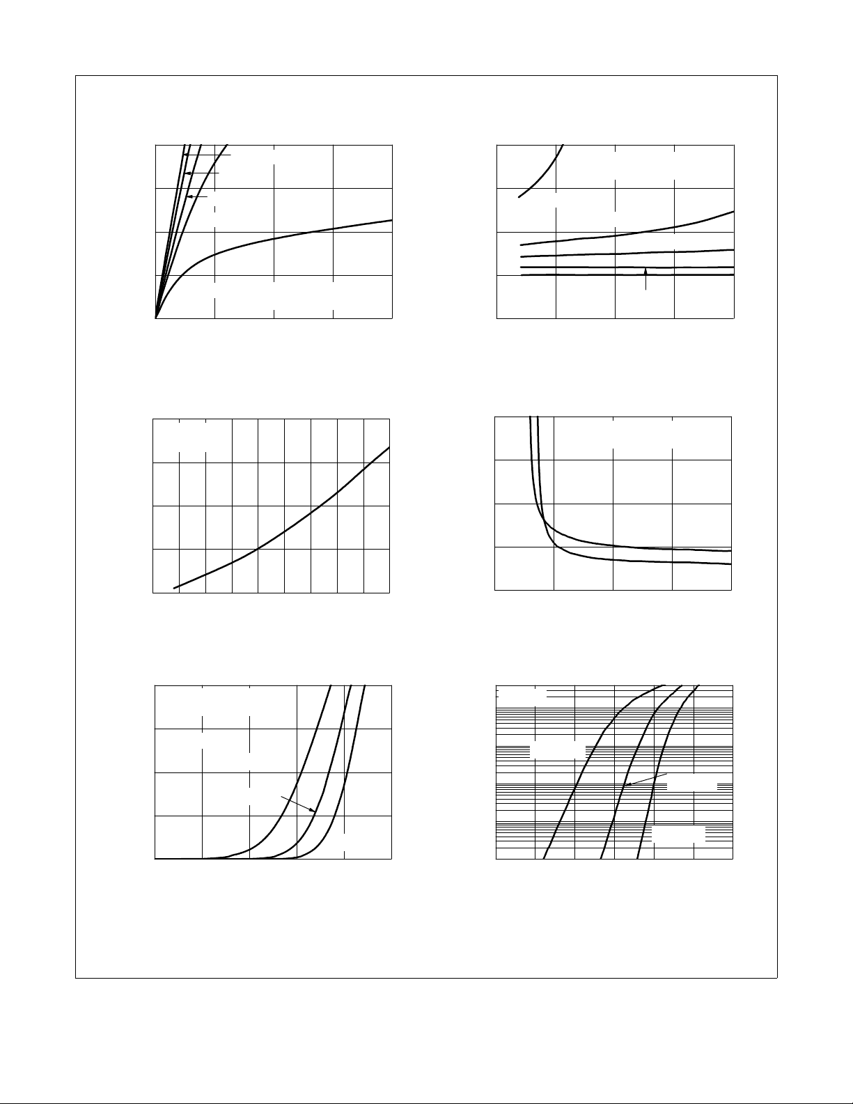
Typical Characteristics (Q1 N-Channel) T
40
30
20
10
, DRAIN CURRENT (A)
D
I
0
VGS = 3.5 V
0.0 0.5 1.0 1.5 2.0
Figure 1.
1.6
ID = 12 A
V
= 10 V
GS
1.4
1.2
NORMALIZED
1.0
DRAIN TO SOURCE ON-RESISTANCE
0.8
-75 -50 -25 0 25 50 75 100 125 150
T
Fi g u r e 3. No r m alized O n Resist a n ce
vs Junction Temperature
VGS = 10 V
V
= 6
V
GS
VGS = 4.5 V
VGS = 4 V
PULSE DURATION = 80 µs
DUTY CYCLE = 0.5% MAX
V
,
DRAIN TO SOURCE VOLTAGE (V)
DS
On Region Characteristics Figure 2.
, JUNCTION TEMPERATURE (
J
o
C)
= 25 °C unless otherwise noted
J
4
3
VGS = 3.5 V
2
NORMALIZED
1
DRAIN TO SOURCE ON-RESISTANCE
0
0 10203040
I
,
D
Norm a l i z e d O n - R e sistance
vs Drain Current and Gate Voltage
40
)
Ω
m
(
30
20
DRAIN TO
,
DS(on)
r
10
SOURCE ON-RESISTANCE
0
246810
Figure 4.
TJ = 125 oC
TJ = 25 oC
V
,
GATE TO SOURCE VOLTAGE (V)
GS
On-Res istance vs Gate to
Source Voltage
PULSE DURATION = 80 µs
DUTY CYCLE = 0.5% MAX
VGS = 4 V
VGS = 6 V
DRAIN CURRENT (A)
PULSE DURATION = 80 µs
DUTY CYCLE = 0.5% MAX
ID = 12 A
V
GS
= 4.5 V
V
= 10 V
GS
®
MOSFET
40
PULSE DURATION = 80 µs
DUTY CYCLE = 0.5% MAX
30
V
= 5 V
DS
20
10
, DRAIN CURRENT (A)
D
I
0
1.5 2.0 2.5 3.0 3.5 4.0
TJ = 150 oC
TJ = 25 oC
VGS, GATE TO SOURCE V OLTAGE (V)
Figure 5. Transfer Characteristics
©2009 Fairchild Semiconductor Corporation
FDMS7600AS Rev.C
40
V
= 0 V
GS
10
1
0.1
0.01
, REVERSE DRAIN CURRENT (A)
S
TJ = -55 oC
I
0.001
0.0 0.2 0.4 0.6 0.8 1.0 1.2
TJ = 150 oC
VSD, BODY DIODE FORWARD VOLTAGE (V)
Figure 6.
Source to Drain Diode
TJ = 25 oC
TJ = -55 oC
Forward Voltage vs Source Current
4
www.fairchildsemi.com