Fairchild FDMS7578 service manual

FDMS7578
N-Channel Power Trench® MOSFET
25 V, 5.8 mΩ
Features
Max r
Max r
Advanced Package and Silicon combination for low r
and high efficiency
Next generation enhanced body diode technology, engineered
for soft recovery
MSL1 robust package design
100% UIL tested
RoHS Compliant
= 5.8 mΩ at VGS = 10 V, ID = 17 A
DS(on)
= 8 mΩ at VGS = 4.5 V, ID = 14 A
DS(on)
DS(on)
General Description
This N-Channel MOSFET has been designed specifically to
improve the overall efficiency and to minimize switch node
ringing of DC/DC converters using either synchronous or
conventional switching PWM controllers. It has been optimized
for low gate charge, low r
diode reverse recovery performance.
Applications
Control MOSFET for Synchronous Buck Converters
Notebook
Server
Telecomm
High Efficiency DC-DC Switch Mode Power Supplies
December 2009
fast switching speed and body
DS(on),
FDMS7578 N-Channel Power Trench
®
MOSFET
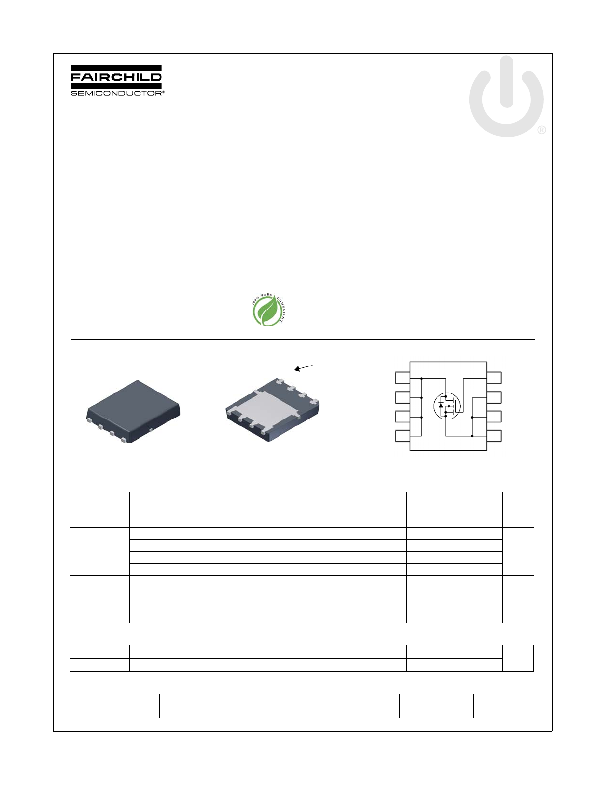
Top
Power 56
D
MOSFET Maximum Ratings T
Symbol Parameter Ratings Units
V
DS
V
GS
I
D
E
AS
P
D
, T
T
J
STG
Drain to Source Voltage 25 V
Gate to Source Voltage (Note 4) ±20 V
Drain Current -Continuous (Package limited) TC = 25 °C 28
-Continuous (Silicon limited) T
-Continuous T
-Pulsed 60
Single Pulse Avalanche Energy (Note 3) 40 mJ
Power Dissipation TC = 25 °C 33
Power Dissipation T
Operating and Storage Junction Temperature Range -55 to +150 °C
Bottom
D
D
D
= 25 °C unless otherwise noted
A
Pin 1
S
S
S
G
= 25 °C 63
C
= 25 °C (Note 1a) 17
A
= 25 °C (Note 1a) 2.5
A
D
5
D
6
D
7
8
D
Thermal Characteristics
G
4
S
3
S
2
S
1
A
W
R
θJC
R
θJA
Thermal Resistance, Junction to Case 3.7
Thermal Resistance, Junction to Ambient (Note 1a) 50
Package Marking and Ordering Information
Device Marking Device Package Reel Size Tape Width Quantity
FDMS7578 FDMS7578 Power 56 13 ’’ 12 mm 3000 units
©2009 Fairchild Semiconductor Corporation
FDMS7578 Rev.C
°C/W
1
www.fairchildsemi.com

FDMS7578 N-Channel Power Trench
Electrical Characteristics T
= 25 °C unless otherwise noted
J
Symbol Parameter Test Conditions Min Typ Max Units
Off Characteristics
BV
DSS
∆BV
DSS
∆T
J
I
DSS
I
GSS
On Characteristics
V
GS(th)
∆V
GS(th)
∆T
J
r
DS(on)
g
FS
Drain to Source Breakdown Voltage ID = 250 µA, VGS = 0 V 25 V
Breakdown Voltage Temperature
Coefficient
Zero Gate Voltage Drain Current VDS = 20 V, V
Gate to Source Leakage Current,Forward VGS = 20 V, V
ID = 250 µA, referenced to 25 °C 20 mV/°C
= 0 V 1 µA
GS
= 0 V 100 nA
DS
Gate to Source Threshold Voltage VGS = VDS, ID = 250 µA 1.0 1.6 3.0 V
Gate to Source Threshold Voltage
Temperature Coefficient
Static Drain to Source On Resistance
Forward Transconductance VDD = 5 V, ID = 17 A 77 S
ID = 250 µA, referenced to 25 °C -6 mV/°C
VGS = 10 V, ID = 17 A 4.6 5.8
VGS = 10 V, ID = 17 A, TJ = 125 °C 6.7 8.5
Dynamic Characteristics
C
iss
C
oss
C
rss
R
g
Input Capacitance
Output Capacitance 371 495 pF
Reverse Transfer Capacitance 54 85 pF
VDS = 13 V, VGS = 0 V,
f = 1 MHz
1221 1625 pF
Gate Resistance 1.2 2.4 Ω
Switching Characteristics
t
d(on)
t
r
t
d(off)
t
f
Q
Q
Q
g(TOT)
gs
gd
Turn-On Delay Time
Rise Time 2.6 10 ns
Turn-Off Delay Time 20 33 ns
VDD = 13 V, ID = 17 A,
VGS = 10 V, R
GEN
= 6 Ω
8 17 ns
Fall Time 2.2 10 ns
Total Gate Charge VGS = 0 V to 10 V
Total Gate Charge VGS = 0 V to 4.5 V 8 11 nC
Total Gate Charge 3.7 nC
VDD = 13 V
ID = 17 A
18 25 nC
Gate to Drain “Miller” Charge 1.7 nC
mΩVGS = 4.5 V, ID = 14 A 6.3 8
®
MOSFET
Drain-Source Diode Characteristics
V
= 0 V, IS = 2 A (Note 2) 0.72 1.1
V
SD
t
rr
Q
rr
t
rr
Q
rr
NOTES:
1. R
is determined with the device mounted on a 1 in2 pad 2 oz copper pad on a 1.5 x 1.5 in. board of FR-4 material. R
θJA
the user's board design.
2. Pulse Test: Pulse Width < 300 µs, Duty cycle < 2.0 %.
3. E
of 40 mJ is based on starting TJ = 25 °C, L = 1 mH, IAS = 9 A, VDD = 23 V, VGS = 10 V. 100% test at L = 0.3 mH, IAS = 14 A.
AS
4. As an N-ch device, the negative Vgs rating is for low duty cycle pulse occurrence only. No continuous rating is implied.
FDMS7578 Rev.C
Source to Drain Diode Forward Voltage
Reverse Recovery Time
Reverse Recovery Charge 6 12 nC
Reverse Recovery Time
Reverse Recovery Charge 13 24 nC
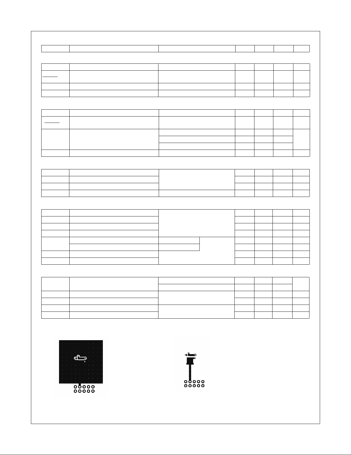
a. 50 °C/W when mounted on
a 1 in2 pad of 2 oz copper
GS
V
= 0 V, IS = 17 A (Note 2) 0.83 1.2
GS
IF = 17 A, di/dt = 100 A/µs
IF = 17 A, di/dt = 300 A/µs
2
20 32 ns
19 34 ns
is guaranteed by design while R
θJC
b.125 °C/W when mounted on
a minimum pad of 2 oz copper
V
is determined by
θCA
www.fairchildsemi.com

FDMS7578 N-Channel Power Trench
Typical Characteristics T
60
45
30
DRAIN CURRENT (A)
15
,
D
I
0
012345
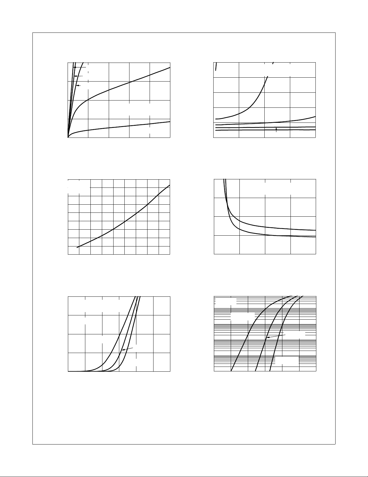
Figure 1.
1.6
1.5
1.4
1.3
1.2
1.1
1.0
NORMALIZED
0.9
0.8
DRAIN TO SOURCE ON-RESISTANCE
0.7
-75 -50 -25 0 25 50 75 100 125 150
Fi gure 3. Norma li ze d O n- Re si stance
VGS = 10 V
VGS = 4.5 V
VGS = 3.5 V
PULSE DURATION = 80 µs
DUTY CYCLE = 0.5% MAX
V
,
DRAIN TO SOURCE VOLTAGE (V)
DS
On-Region Characteristics Figure 2.
ID = 17 A
= 10 V
V
GS
T
,
JUNCTION TEMPERATUR E
J
vs Junction Temperature
= 25 °C unless otherwise noted
J
VGS = 3 V
VGS = 2.5 V
o
(
C
)
10
VGS = 2.5 V
8
VGS = 3 V
PULSE DURATION = 80 µs
DUTY CYCLE = 0.5% MAX
6
4
NORMALIZED
VGS = 3.5 V
2
DRAIN TO SOURCE ON-RESISTA NC E
0
0 15304560
I
,
DRAIN CURRENT (A)
D
VGS = 4.5 V
VGS = 10 V
Norma li zed On -R esist an ce
vs Drain Current and Gate Voltage
20
)
Ω
m
(
15
10
DRAIN TO
,
DS(on)
r
5
SOURCE ON-RESISTANCE
0
246810
Figure 4.
ID = 17 A
V
, GATE TO S OURCE VOLTAG E ( V )
GS
On-Resistance vs Gat e to
PULSE DURATION = 80 µs
DUTY CYCLE = 0.5% MAX
TJ = 125 oC
TJ = 25 oC
Source Voltage
®
MOSFET
60
45
30
15
, DRAIN CURRENT (A)
D
I
FDMS7578 Rev.C
PULSE DURATION = 80 µs
DUTY CYCLE = 0.5% MAX
V
= 5 V
DS
TJ = 150 oC
TJ = 25 oC
TJ = -55 oC
0
1.0 1.5 2.0 2.5 3.0 3.5 4.0
VGS, GATE TO SOURCE V OLTAGE (V)
Figure 5. Transfer Characteristics
60
V
= 0 V
GS
10
TJ = 150 oC
1
0.1
0.01
, REVERSE DRAIN CURRENT (A)
S
I
0.001
0.0 0.2 0.4 0.6 0.8 1.0 1.2
VSD, BODY DIODE FORWARD VOLTAGE (V)
Figure 6.
Sou rce to Drain Diode
TJ = 25 oC
TJ = -55 oC
Forward Voltage vs Source Current
3
www.fairchildsemi.com
 Loading...