

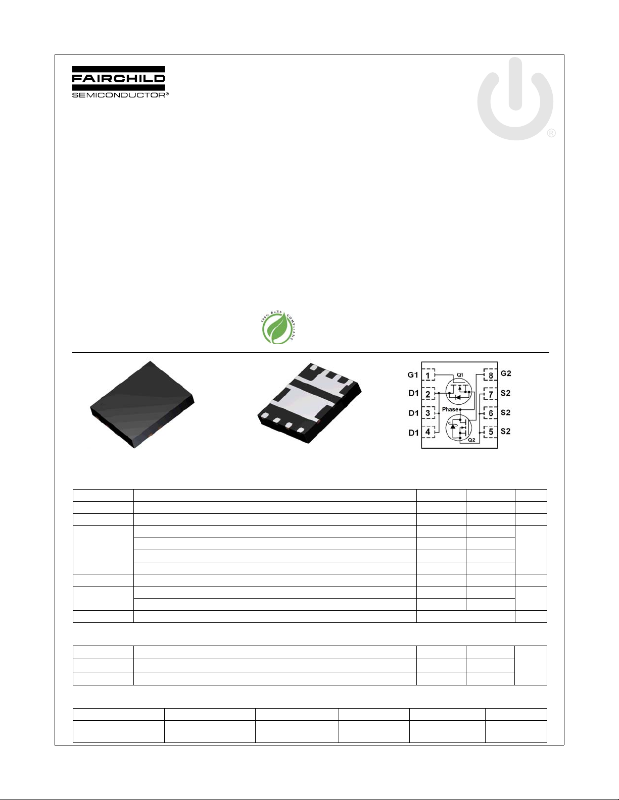
FDMS3686S
Power 56
G1
D1
D1
D1
G2
S2
S2
S2
D1
PHASE
(S1/D2)
Top Bottom
PowerTrench® Power Stage
Asymmetric Dual N-Channel MOSFET
Features
Q1: N-Channel
Max r
Max r
Q2: N-Channel
Max r
Max r
Low inductance packaging shortens rise/fall times, resulting in
lower switching losses
MOSFET integration enables optimum layout for lower circuit
inductance and reduced switch node ringing
RoHS Compliant
= 8 mΩ at VGS = 10 V, ID = 13 A
DS(on)
= 11 mΩ at VGS = 4.5 V, ID = 11 A
DS(on)
= 2.8 mΩ at VGS = 10 V, ID = 23 A
DS(on)
= 3.8 mΩ at VGS = 4.5 V, ID = 21 A
DS(on)
General Description
This device includes two specialized N-Channel MOSFETs in a
dual PQFN package. The switch node has been internally
connected to enable easy placement and routing of synchronous
buck converters. The control MOSFET (Q1) and synchronous
SyncFET (Q2) have been designed to provide optimal power
efficiency.
Applications
Computing
Communications
General Purpose Point of Load
Notebook VCORE
January 2012
FDMS3686S PowerTrench
®
Power Stage
MOSFET Maximum Ratings T
Symbol Parameter Q1 Q2 Units
V
DS
V
GS
I
D
E
AS
P
D
TJ, T
STG
Thermal Characteristics
R
θJA
θJA
R
θJC
Package Marking and Ordering Information
Device Marking Device Package Reel Size Tape Width Quantity
©2012 Fairchild Semiconductor Corporation
FDMS3686S Rev.C1
Drain to Source Voltage 30 30 V
Gate to Source Voltage (Note 3) ±20 ±20 V
Drain Current -Continuous (Package limited) TC = 25 °C 30 55
-Continuous (Silicon limited) T
-Continuous T
-Pulsed 40 100
Single Pulse Avalanche Energy 40
Power Dissipation for Single Operation TA = 25 °C 2.2
Power Dissipation for Single Operation T
Operating and Storage Junction Temperature Range -55 to +150 °C
Thermal Resistance, Junction to Ambient 57
Thermal Resistance, Junction to Ambient 125
Thermal Resistance, Junction to Case 3.5 2.0
22CA
F10CC
FDMS3686S Power 56 13 ” 12 mm 3000 units
= 25 °C unless otherwise noted
A
1
= 25 °C 54 123
C
= 25 °C 13
A
= 25 °C 1.0
A
1a
4
1a
1c
1a
1c
1b
23
4
60
1b
2.5
1d
1.0
1b
50
1d
120
www.fairchildsemi.com
A
mJ
W
°C/WR
FDMS3686S PowerTrench
Electrical Characteristics T
= 25 °C unless otherwise noted
J
Symbol Parameter Test Conditions Type Min Typ Max Units
Off Characteristics
BV
ΔBV
ΔT
I
DSS
I
GSS
DSS
DSS
J
= 250 μA, VGS = 0 V
Drain to Source Breakdown Voltage
Breakdown Voltage Temperature
Coefficient
D
I
= 1 mA, VGS = 0 V
D
ID = 250 μA, referenced to 25 °C
I
= 10 mA, referenced to 25 °C
D
Zero Gate Voltage Drain Current VDS = 24 V, V
Gate to Source Leakage Current,
Forwad
V
= 20 V, VDS= 0 V
GS
GS
= 0 V
Q1Q230
30
Q1
Q2
Q1
Q2
Q1
Q2
V
15
19
500
100
100
mV/°C
1
I
On Characteristics
V
V
GS(th)
ΔV
ΔT
r
DS(on)
g
FS
GS(th)
J
Gate to Source Threshold Voltage
Gate to Source Threshold Voltage
Temperature Coefficient
Drain to Source On Resistance
Forward Transconductance
= VDS, ID = 250 μA
GS
V
= VDS, ID = 1 mA
GS
ID = 250 μA, referenced to 25 °C
I
= 10 mA, referenced to 25 °C
D
= 10 V, ID = 13 A
V
GS
V
= 4.5 V, ID = 11 A
GS
V
= 10 V , ID = 13 A , TJ = 125 °C
GS
V
= 10 V, ID = 23 A
GS
V
= 4.5 V, ID = 21 A
GS
V
= 10 V , ID = 23 A , TJ = 125 °C
GS
V
= 5 V, ID = 13 A
DS
V
= 5 V, ID = 23 A
DS
Q1Q21.1
1.121.5
Q1
Q2
Q1
Q2
Q1
Q2
-6
-4
5.8
8.5
7.8
2.2
3.0
3.1
61
124
2.7
3.0
mV/°C
8
11
10.8
2.8
3.8
4.0
μA
μA
nA
nA
V
mΩ
S
®
Power Stage
Dynamic Characteristics
C
iss
C
oss
C
rss
R
g
Input Capacitance
Output Capacitance
Reverse Transfer Capacitance
Gate Resistance
Switching Characteristics
t
d(on)
t
r
t
d(off)
t
f
Q
Q
Q
Q
g
g
gs
gd
Turn-On Delay Time
Rise Time
Turn-Off Delay Time
Fall Time
Total Gate Charge V
Total Gate Charge V
Gate to Source Gate Charge
Gate to Drain “Miller” Charge
1340
Q1:
= 15 V, VGS = 0 V, f = 1 MHZ
V
DS
Q2:
= 15 V, VGS = 0 V, f = 1 MHZ
V
DS
Q1
Q2
Q1
Q2
Q1
Q2
Q1Q20.2
0.2
1820
485
725
53
8680130
0.6
0.9
1785
2420
645
965
2
3
pF
pF
pF
Ω
8.2916
18
2.5410
10
20
23
32
36
2.2310
10
21
27
10
13
29
37
14
18
3.9
4.6
3.1
3.7
ns
ns
ns
ns
nC
nC
nC
nC
Q1:
= 15 V, ID = 13 A, R
V
DD
Q2:
= 15 V, ID = 23 A, R
V
DD
= 0 V to 10 V
GS
= 0 V to 4.5 V
GS
= 6 Ω
GEN
= 6 Ω
GEN
Q1
V
= 15 V,
DD
I
= 13 A
D
Q2
VDD = 15 V,
I
= 23 A
D
Q1
Q2
Q1
Q2
Q1
Q2
Q1
Q2
Q1
Q2
Q1
Q2
Q1
Q2
Q1
Q2
©2012 Fairchild Semiconductor Corporation
FDMS3686S Rev.C1
2
www.fairchildsemi.com
FDMS3686S PowerTrench
Electrical Characteristics T
= 25 °C unless otherwise noted
J
Symbol Parameter Test Conditions Type Min Typ Max Units
Drain-Source Diode Characteristics
1.2
V
= 0 V, IS = 2 A (Note 2)
GS
V
= 0 V, IS = 13 A (Note 2)
V
SD
t
rr
Q
rr
Notes:
1. R
is determined with the device mounted on a 1 in2 pad 2 oz copper pad on a 1.5 x 1.5 in. board of FR-4 material. R
qJA
by the user's board desi gn.
Source to Drain Diode Forward Voltage
Reverse Recovery Time
Reverse Recovery Charge
a. 57 °C/W when mounted on
2
a 1 in
pad of 2 oz copper
SS
SF
DF
DS
G
GS
V
= 0 V, IS = 2 A (Note 2)
GS
V
= 0 V, IS = 23 A (Note 2)
GS
Q1
I
= 13 A, di/dt = 100 A/μs
F
Q2
I
= 23 A, di/dt = 300 A/μs
F
DS
DF
G
SF
SS
Q1
Q1
Q2
Q2
Q1
Q2
Q1
Q2
is guaranteed by design while R
qJC
b. 50 °C/W when mounted on
2
pad of 2 oz copper
a 1 in
0.72
1.2
0.82
0.58
0.76
25
25
9
23
1.2
1.2
40
39
18
36
is determined
qCA
V
ns
nC
®
Power Stage
c. 125 °C/W when mounted on a
minimum pad of 2 oz copper
SF
SS
DS
DF
SS
SF
DF
DS
G
2. Pulse Test: Pulse Width < 300 ms, Duty cycle < 2.0%.
3. As an N-ch device, the negative Vgs rating is for low duty cycle pulse ocurrence only. No continuous rating is implied.
4. Q1: EAS of 40 mJ is based on starting TJ = 25 oC; N-ch: L = 1 mH, IAS = 9 A, VDD = 27 V, VGS = 10 V. 100% test at L= 0.3 mH, IAS = 14 A.
of 60 mJ is based on starting TJ = 25 oC; N-ch: L = 1 mH, IAS = 11 A, VDD = 27 V, VGS = 10 V. 100% test at L= 0.3 mH, IAS = 17 A.
Q2: E
AS
G
d. 120 °C/W when mounted on a
minimum pad of 2 oz copper
©2012 Fairchild Semiconductor Corporation
FDMS3686S Rev.C1
3
www.fairchildsemi.com
FDMS3686S PowerTrench
0.0 0.2 0.4 0.6 0.8 1.0
0
10
20
30
40
VGS = 4.5 V
VGS = 3.5 V
V
GS
= 6 V
VGS = 4 V
PULSE DURATION = 80 μs
DUTY CYCLE = 0.5% MAX
VGS = 10 V
I
D
, DRAIN CURRENT (A)
V
DS
, DRAIN TO SOURCE VOLTAGE (V)
0 10203040
0
1
2
3
4
VGS = 6 V
VGS = 3.5 V
PULSE DURA TION = 80 μs
DUTY CYCLE = 0.5% MAX
NORMALIZED
DRAIN TO SOURCE ON-RESISTA NCE
I
D
, DRAIN CURRENT (A)
V
GS
= 4 V
VGS = 4.5 V
V
GS
= 10 V
-75 -50 -25 0 25 50 75 100 125 150
0.6
0.8
1.0
1.2
1.4
1.6
ID = 13 A
V
GS
= 10 V
NORMALIZED
DRAIN TO SOURCE ON-RESISTANCE
T
J
, JUNCTION TE MPERATURE (
o
C)
246810
0
4
8
12
16
20
TJ = 125 oC
ID = 13 A
TJ = 25 oC
V
GS
, GATE TO SOURCE VOLTA GE (V)
r
DS(on)
,
DRAIN TO
SOURCE ON-RESISTANCE
(mΩ)
PULSE DURATION = 80 μs
DUTY CYCLE = 0.5% MAX
1.5 2.0 2.5 3.0 3.5 4.0
0
10
20
30
40
TJ = 150 oC
V
DS
= 5 V
PULSE DURATION = 80 μs
DUTY CYCLE = 0.5% MAX
TJ = -55 oC
TJ = 25 oC
I
D
, DRAIN CURRENT (A)
VGS, GATE TO SOURCE VOLTAGE (V)
0.0 0.2 0.4 0.6 0.8 1.0 1.2
0.001
0.01
0.1
1
10
40
TJ = -55 oC
TJ = 25 oC
TJ = 150 oC
V
GS
= 0 V
I
S
, REVERSE DRAIN CURRENT (A)
VSD, BODY DIODE FORWARD VOLTAGE (V)
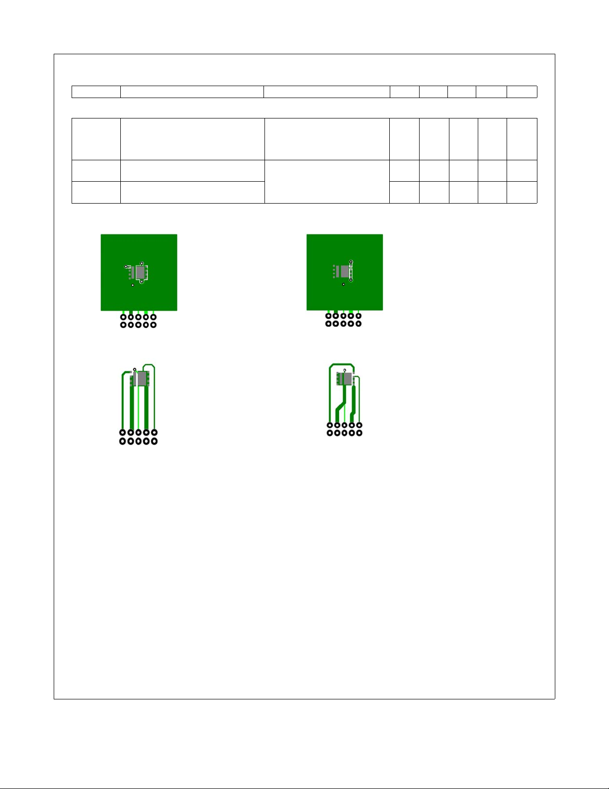
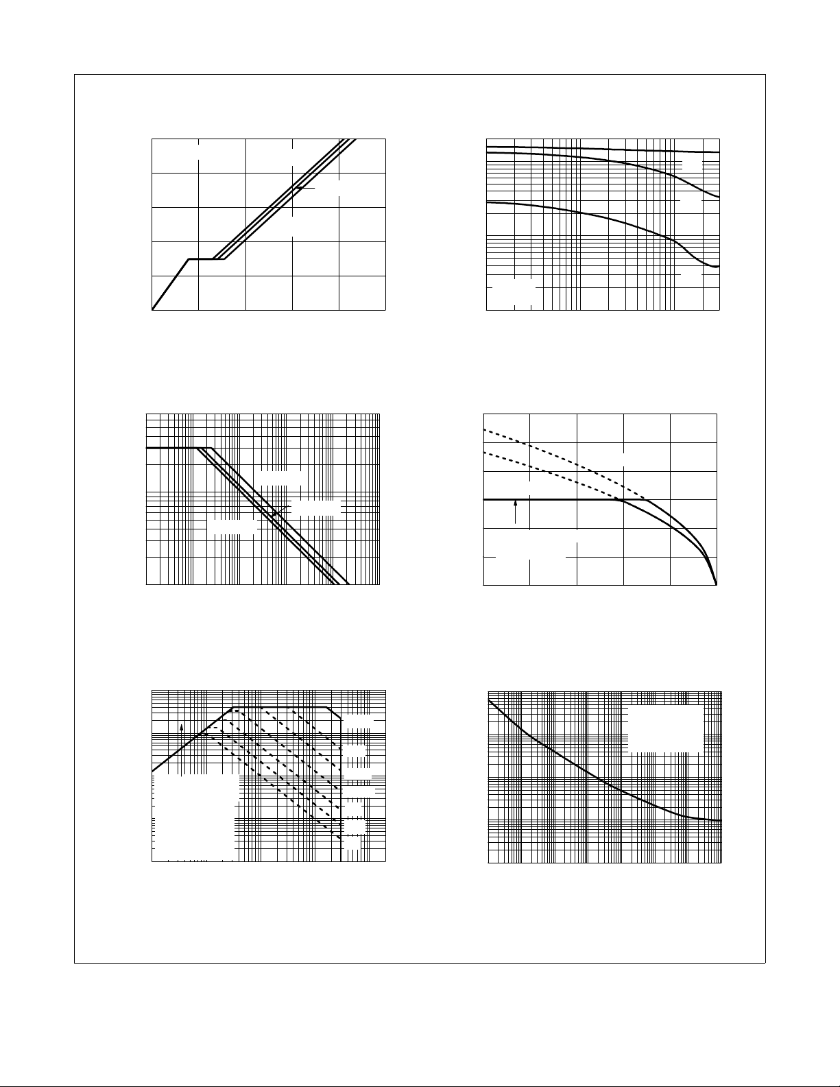
Typical Characteristics (Q1 N-Channel) T
Figure 1.
On Region Characteristics Figure 2.
= 25 °C unless otherwise noted
J
Norm a l i z e d O n - R e sistance
vs Drain Current and Gate Voltage
®
Power Stage
Fi g u r e 3. No r m alized O n Resist a n ce
vs Junction Temperature
©2012 Fairchild Semiconductor Corporation
FDMS3686S Rev.C1
Figure 5. Transfer Characteristics
Figure 4.
On-Res istance vs Gate to
Source Voltage
Figure 6.
Source to Drain Diode
Forward Voltage vs Source Current
4
www.fairchildsemi.com
FDMS3686S PowerTrench
0 5 10 15 20 25
0
2
4
6
8
10
ID = 13 A
V
DD
= 20 V
V
DD
= 10 V
V
GS
, GATE TO SOURCE VOLTAGE (V)
Qg, GATE CHARGE (nC)
VDD = 15 V
0.1 1 10 30
10
100
1000
2000
f = 1 MHz
V
GS
= 0 V
CAPACITANCE (pF)
VDS, DRAIN TO SOURCE VOLTAGE (V)
C
rss
C
oss
C
iss
0.001 0.01 0.1 1 10 100
1
10
70
TJ = 100 oC
TJ = 25 oC
TJ = 125 oC
tAV, TIME IN AVALANCHE (ms)
I
AS
, AVALANCHE CURRENT (A)
25 50 75 100 125 150
0
10
20
30
40
50
60
R
θJC
= 3.5 oC/W
V
GS
= 4.5 V
Limited by P ackage
V
GS
= 10 V
I
D
, DRAIN CURRENT (A)
T
A
, AMBIENT TEMPERATURE (
o
C)
0.01 0.1 1 10 100
0.01
0.1
1
10
100
DC
100 ms
10 ms
1 ms
1s
I
D
, DRAIN CURRENT (A)
VDS, DRAIN to SOURCE VOLTAGE (V)
THIS AREA IS
LIMITED BY r
DS(on)
SINGLE PULSE
T
J
= MAX RATED
R
θJA
= 125
o
C/W
T
A
= 25
o
C
10s
100us
200
10-410-310-210
-1
110
100 1000
0.1
1
10
100
1000
SINGLE PULSE
R
θJA
= 125
o
C/W
T
A
= 25
o
C
P(
PK
), PEAK TRANSIENT POWER (W)
t, PULSE WIDTH (sec)
Typical Characteristics (Q1 N-Channel) T
Figure 7.
Gate Charge Characteristics Figure 8.
= 25 °C unless otherwise noted
J
Capa c i t a nce v s D r ain
to Source Voltage
®
Power Stage
Figure 9.
Un c l a mp e d I nd u c tiv e
Switching Capability
©2012 Fairchild Semiconductor Corporation
FDMS3686S Rev.C1
Figure 11. Forward Bias Safe
Op
erating Area
Figure 10.
Maximum Continuous Drain
Current vs Case Temperature
Figure 12. Single Pulse Maximum
Power Dissipation
5
www.fairchildsemi.com

FDMS3686S PowerTrench
10
-4
10
-3
10
-2
10
-1
110
100 1000
0.001
0.01
0.1
1
SINGLE PULSE
R
θJA
= 125 oC/W
(Note 1c)
DUTY CYCLE-DESCENDING ORDER
NORMALIZED THERMAL
IMPEDANCE,
Z
θJA
t, RECTANGULAR PU L SE D U R ATION (sec)
D = 0.5
0.2
0.1
0.05
0.02
0.01
2
P
DM
t
1
t
2
NOTES:
DUTY FACTOR: D = t1/t
2
PEAK TJ = PDM x Z
θJA
x R
θJA
+ T
A
Typical Characteristics (Q1 N-Channel) T
Figure 13. Junction-to-Ambient Transient Thermal Response Curve
= 25 °C unless otherwise noted
J
®
Power Stage
©2012 Fairchild Semiconductor Corporation
FDMS3686S Rev.C1
6
www.fairchildsemi.com
FDMS3686S PowerTrench
0.00.20.40.60.81.0
0
20
40
60
80
100
VGS = 4.5 V
VGS = 3 V
V
GS
= 3.5 V
VGS = 4 V
PULSE DURATION = 80 μs
DUTY CYCLE = 0.5% MAX
VGS = 10 V
I
D
, DRAIN CURRENT (A)
V
DS
, DRAIN TO SOURCE VOLTAGE (V)
0 20406080100
0
1
2
3
4
VGS = 3 V
VGS = 3.5 V
PULSE DURATION = 80 μs
DUTY CYCLE = 0.5% MAX
NORMALIZED
DRAIN TO SOURCE ON-RESISTA NCE
I
D
, DRAIN CURRENT (A)
V
GS
= 4 V
VGS = 4.5 V
V
GS
= 10 V
-75 -50 -25 0 25 50 75 100 125 150
0.6
0.8
1.0
1.2
1.4
1.6
ID = 23 A
V
GS
= 10 V
NORMALIZED
DRAIN TO SOURCE ON-RESISTANCE
T
J
, JUNCTION TE MPERATURE (
o
C)
246810
0
3
6
9
12
TJ = 125 oC
ID = 23 A
TJ = 25 oC
V
GS
, GATE TO SOURCE VOLTA G E (V)
r
DS(on)
,
DRAIN TO
SOURCE ON-RESISTANCE
(mΩ)
PULSE DURA TION = 80 μs
DUTY CYCLE = 0.5% MAX
1.52.02.53.03.54.0
0
20
40
60
80
100
TJ = 125 oC
V
DS
= 5 V
PULSE DURATION = 80 μs
DUTY CYCLE = 0.5% MAX
TJ = -55 oC
TJ = 25 oC
I
D
, DRAIN CURRENT (A)
VGS, GATE TO SOURCE VOLTAGE (V)
0.0 0.2 0.4 0.6 0.8 1.0 1.2
0.001
0.01
0.1
1
10
100
TJ = -55 oC
TJ = 25 oC
TJ = 125 oC
V
GS
= 0 V
I
S
, REVERSE DRAIN CURRENT (A)
VSD, BODY DIODE FORWARD VOLTAGE (V)
Typical Characteristics (Q2 N-Channel) T
Figure 14. On-Region Characteristics
= 25 oC unlenss otherwise noted
J
Figure 15. Normalized on-Resistance vs Drain
Current and Gate V oltage
®
Power Stage
Figure 16. Normalized On-Resistance
vs Junction Temperature
©2012 Fairchild Semiconductor Corporation
FDMS3686S Rev.C1
Figure 18. Transfer Characteristics
Figure 17. On-Resistance vs Gate to
Source Voltage
Figure 19. Source to Drain Diode
Forward Voltage vs Source Current
7
www.fairchildsemi.com

0 5 10 15 20 25 30
0
2
4
6
8
10
ID = 23 A
V
DD
= 20 V
V
DD
= 10 V
V
GS
, GATE TO SOURCE VOLTAGE (V)
Qg, GATE CHARGE (nC)
VDD = 15 V
0.1 1 10 30
10
100
1000
10000
f = 1 MHz
V
GS
= 0 V
CAPACITANCE (pF)
VDS, DRAIN TO SOURCE VOLTAGE (V)
C
rss
C
oss
C
iss
0.001 0.01 0.1 1 10 100
1
10
70
TJ = 100 oC
TJ = 25 oC
TJ = 125 oC
tAV, TIME IN AVALANCHE (ms)
I
AS
, AVALANCHE CURRENT (A)
25 50 75 100 125 150
0
40
80
120
160
R
θJC
= 2.0 oC/W
V
GS
= 4.5 V
Limited by Package
V
GS
= 10 V
I
D
, DRAIN CURRENT (A)
T
C
, CASE TEMPERATURE (
o
C)
FDMS3686S PowerTrench
0.01 0.1 1 10 100200
0.01
0.1
1
10
100
200
100 us
DC
100 ms
10 ms
1 ms
1s
I
D
, DRAIN CURRENT (A)
VDS, DRAIN to SOURCE VOLTAGE (V)
THIS A REA IS
LIMITED BY r
DS(on)
SINGLE PULSE
T
J
= MAX RATED
R
θJA
= 120
o
C/W
T
A
= 25
o
C
10s
10-410-310-210
-1
110
100 1000
0.1
1
10
100
1000
10000
SINGLE PULSE
R
θJA
= 120
o
C/W
T
A
= 25
o
C
P(
PK
), PEAK TRANSIENT POWER (W)
t, PULSE WIDTH (sec)
Typical Characteristics (Q2 N-Channel) T
Figure 20. Gate Charge Characteristics
o
= 25
C unless otherwise noted
J
Figure 21. Capacitance vs Drain
to Source Voltage
®
Power Stage
Figure 22. Unclamped Inductive
Swit
ching Capability
©2012 Fairchild Semiconductor Corporation
FDMS3686S Rev.C1
Figure 24. Forward Bias Safe
ating Area
Oper
Figure 23. Maximun Continuous Drain
Current vs Case Temperature
Figure 25. Single Pulse Maximum
Power Di
8
ssipation
www.fairchildsemi.com

FDMS3686S PowerTrench
Figure 26. Junction-to-Ambient Transient Thermal Response Curve
10
-4
10
-3
10
-2
10
-1
110
100 1000
0.0001
0.001
0.01
0.1
1
2
SINGLE PULSE
R
θJA
= 120 oC/W
(Note 1d)
DUTY CYCLE-DESCENDING ORDER
NORMALIZED THERMAL
IMPEDANCE,
Z
θJA
t, RECTANGULAR PULSE DURATION (sec)
D = 0.5
0.2
0.1
0.05
0.02
0.01
P
DM
t
1
t
2
NOTES:
DUTY FACTOR: D = t
1/t2
PEAK TJ = PDM x Z
θJA
x R
θJA
+ T
A
Typical Characteristics (Q2 N-Channel) T
= 25 oC unless otherwise noted
J
®
Power Stage
©2012 Fairchild Semiconductor Corporation
FDMS3686S Rev.C1
9
www.fairchildsemi.com
0 50 100 150 200
-5
0
5
10
15
20
25
didt = 300 A/μs
CURRENT (A)
TIME (ns)
Typical Characteristics (continued)
0 5 10 15 20 25 30
10
-6
10
-5
10
-4
10
-3
10
-2
TJ = 125 oC
TJ = 100 oC
TJ = 25 oC
I
DSS
, REVERSE LEAKAGE CURRENT (A)
VDS, REVERSE VOLTAGE (V)
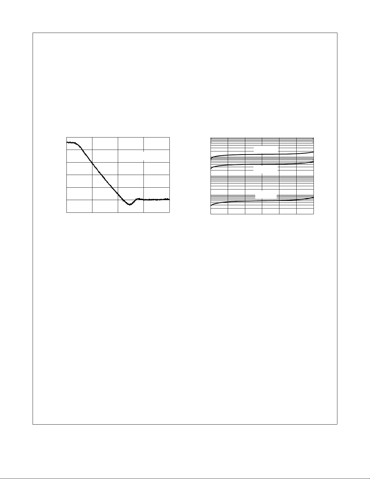
SyncFET Schottky body diode
Characteristics
FDMS3686S PowerTrench
Fairchild’s SyncFET process embeds a Schottky diode in parallel
with PowerTrench MOSFET. This diode exhibits similar
characteristics to a discrete external Schottky diode in parallel
with a MOSFET. Figure 27 shows the reverse recovery
characteristic of the FDMS3686S.
Figure 27. FDMS3686S SyncFET body
diode reverse recovery characteristic
Schottky barrier diodes exhibit significant leakage at high temperature and high reverse voltage. This will increase the power
in the device.
Figure 28. SyncFET body diode reverse
leakage versus drain-source voltage
®
Power Stage
©2012 Fairchild Semiconductor Corporation
FDMS3686S Rev.C1
10
www.fairchildsemi.com
Application Information
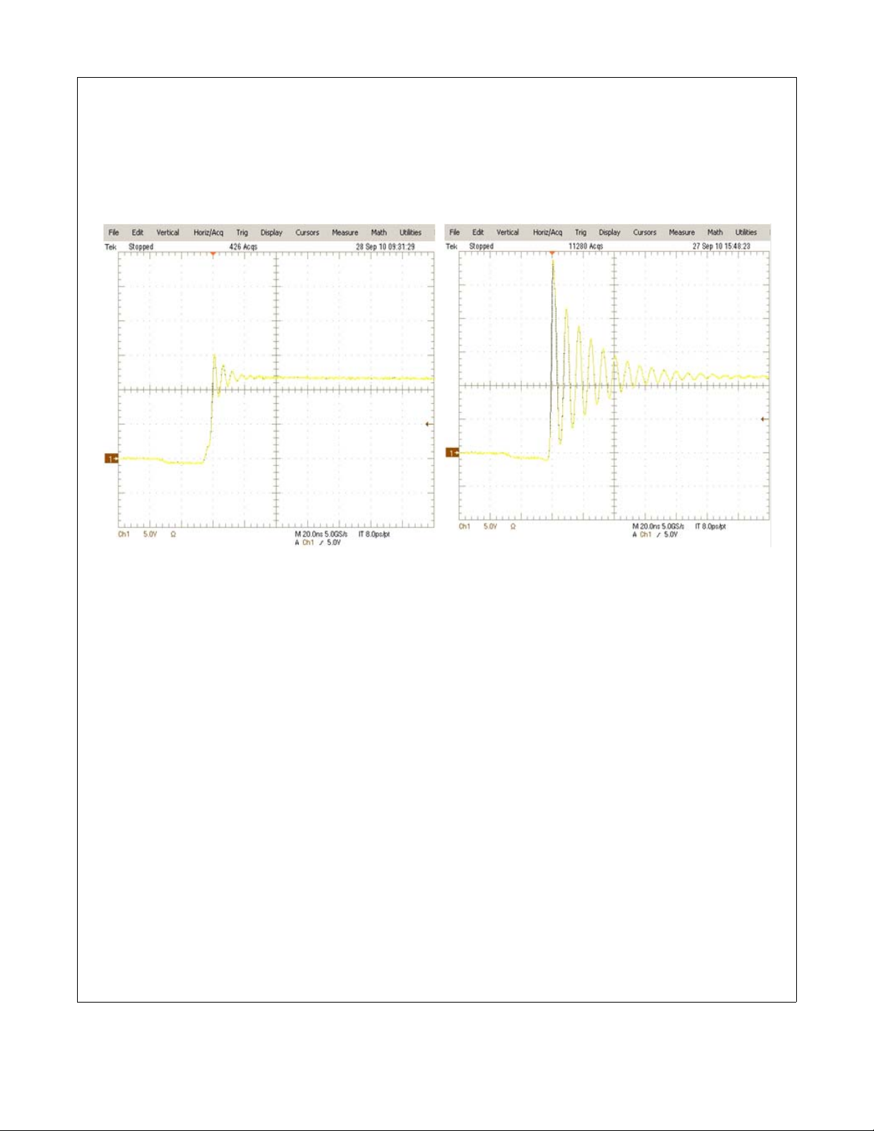
1. Switch Node Ringing Suppression
Fairchild’s Power Stage products incorporate a proprietary design* that minimizes the peak overshoot, ringing voltage on the switch
node (PHASE) without the need of any external snubbing components in a buck converter. As shown in the figure 29, the Power Stage
solution rings significantly less than competitor solutions under the same set of test conditions.
FDMS3686S PowerTrench
®
Power Stage
Power Stage Device
Competitors solution
Figure 29. Power Stage phase node rising edge, High Side Turn on
*Patent Pending
©2012 Fairchild Semiconductor Corporation
FDMS3686S Rev.C1
11
www.fairchildsemi.com

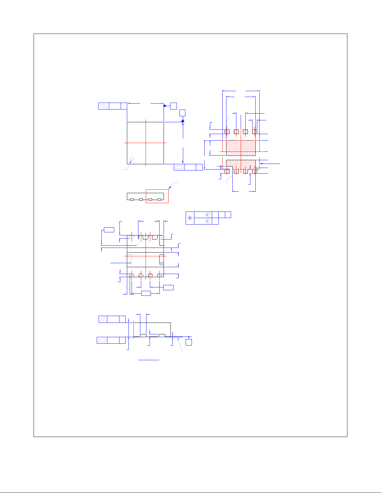
Figure 30. Shows the Power Stage in a buck converter topology
FDMS3686S PowerTrench
®
Power Stage
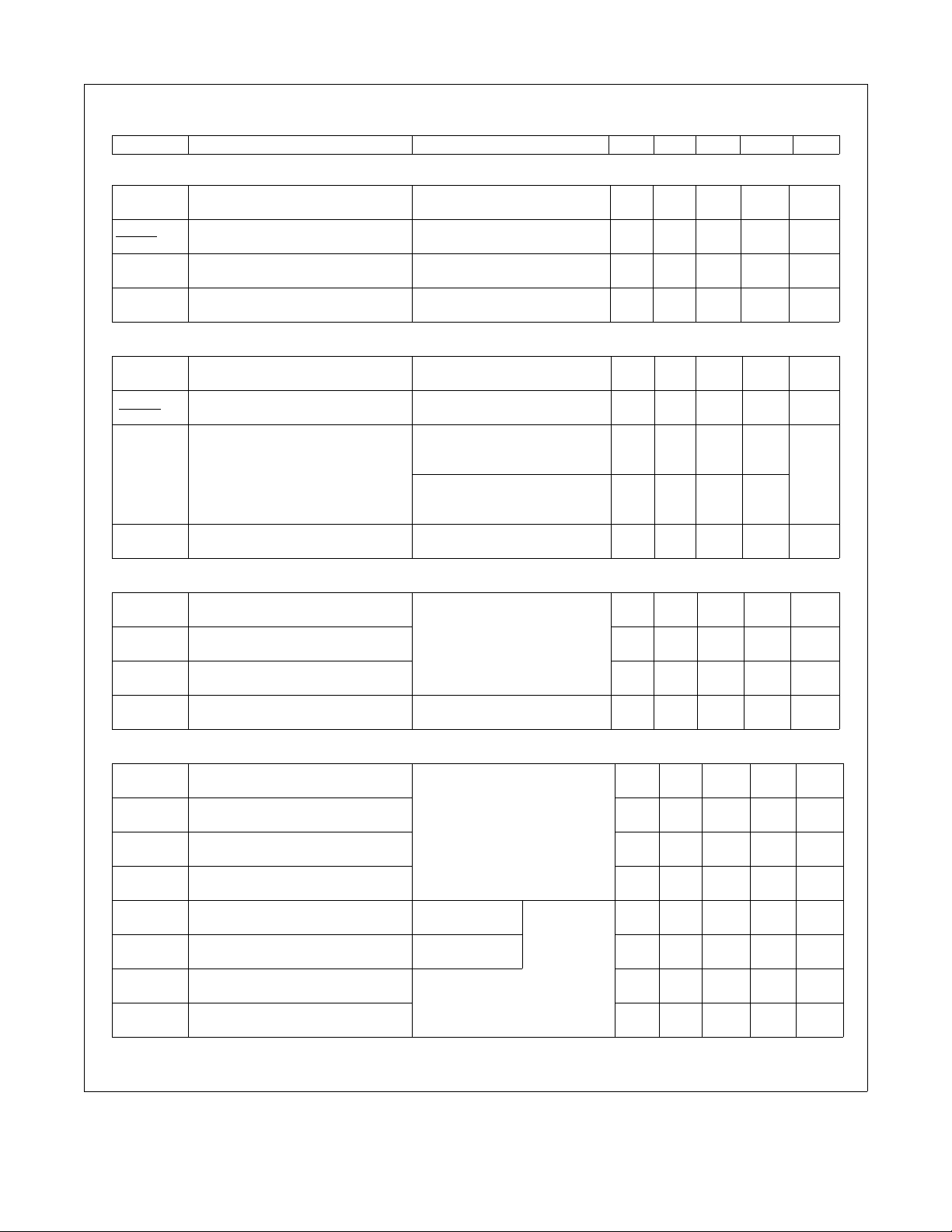
2. Recommended PCB Layout Guidelines
As a PCB designer, it is necessary to address critical issues in layout to minimize losses and optimize the performance of the power
train. Power Stage is a high power density solution and all high current flow paths, such as VIN (D1), PHASE (S1/D2) and GND (S2),
should be short and wide for better and stable current flow, heat radiation and system performance. A recommended layout procedure is discussed below to maximize the electrical and thermal performance of the part.
Figure 31. Recommended PCB Layout
©2012 Fairchild Semiconductor Corporation
FDMS3686S Rev.C1
12
www.fairchildsemi.com

Following is a guideline, not a requirement which the PCB designer should consider:
1. Input ceramic bypass capacitors C1 and C2 must be placed close to the D1 and S2 pins of Power Stage to help reduce parasitic
inductance and High Frequency conduction loss induced by switching operation. C1 and C2 show the bypass capacitors placed close
to the part between D1 and S2. Input capacitors should be connected in parallel close to the part. Multiple input caps can be connected
depending upon the application.
2. The PHASE copper trace serves two purposes; In addition to being the current path from the Power Stage package to the output
inductor (L), it also serves as heat sink for the lower FET in the Power Stage package. The trace should be short and wide enough to
present a low resistance path for the high current flow between the Power Stage and the inductor. This is done to minimize conduction
losses and limit temperature rise. Please note that the PHASE node is a high voltage and high frequency switching node with high
noise potential. Care should be taken to minimize coupling to adjacent traces. The reference layout in figure 31 shows a good balance
between the thermal and electrical performance of Power Stage.
3. Output inductor location should be as close as possible to the Power Stage device for lower power loss due to copper trace
resistance. A shorter and wider PHASE trace to the inductor reduces the conduction loss. Preferably the Power Stage should be
directly in line (as shown in figure 31) with the inductor for space savings and compactness.
4. The PowerTrench
part to operate well within the breakdown voltage limits. This eliminates the need to have an external snubber circuit in most cases. If
the designer chooses to use an RC snubber, it should be placed close to the part between the PHASE pad and S2 pins to dampen
the high-frequency ringing.
5. The driver IC should be placed close to the Power Stage part with the shortest possible paths for the High Side gate and Low Side
gates through a wide trace connection. This eliminates the effect of parasitic inductance and resistance between the driver and the
MOSFET and turns the devices on and off as efficiently as possible. At higher-fre quency opera tion this imp edance can limit the gate
current trying to charge the MOSFET input capacitance. This will result in slower rise and fall times and additional sw itching losses.
Power Stage has both the gate pins on the same side of the package which allows for back mounting of the driver IC to the board. This
provides a very compact path for the drive signals and improves efficiency of the part.
®
Technology MOSFETs used in the Power Stage are effective at minimizing phase node ringing. It allows the
FDMS3686S PowerTrench
®
Power Stage
6. S2 pins should be connected to the GND plane with multiple vias for a low impedance grounding. Poor grounding can create a noise
transient offset voltage level between S2 and driver ground. This could lead to faulty operation of the gate driver and MOSFET.
7. Use multiple vias on each copper area to interconnect top, inner and bottom layers to help smooth current flow and heat conduction.
Vias should be relatively large, around 8 mils to 10 mils, and of reasonable inductance. Critical high frequency components such as
ceramic bypass caps should be located close to the part and on the same side of the PCB. If not feasible, they should be connected
from the backside via a network of low inductance vias.
©2012 Fairchild Semiconductor Corporation
FDMS3686S Rev.C1
13
www.fairchildsemi.com
Dimensional Outline and Pad Layout
C
L
L
CPKG
PKG
5.10
4.90
6.10
5.90
C
3.00
2.80
3.81
1.02
0.82
TOP VIEW
SIDE VIEW
BOTTOM VIEW
14
85
123
4
876
0.10 CAB
0.05
C
2.25
2.05
5
0.58
0.38
NOTES : UNLE SS OTHERWISE SPECIFIED
A) DOES NOT FULLY CONFORM TO
JEDE C REGIS TRATION, MO-240,
ISSUE B DATED 10/2009.
B) ALL DIMENSIONS ARE IN
MILLIMETERS.
C) DIME NSIONS DO NOT INCLUDE
BURRS OR MOLD FLASH. MOLD
FLASH OR BURRS DOES NOT
EXCEED 0.10MM.
D) DIME NSIONING AND TOLE RANCING
PER ASME Y14.5M-1994.
E) IT IS RECOMMENDED TO HAVE NO
TRACES OR VIAS WITHIN T H E KEEP
OUT AREA.
F) DRAWING FILE NAME: PQN08EREV4.
SEE
DETAIL A
DETAIL A
(SCALE: 2X)
0.05
0.00
0.30
0.20
0.08
C
PIN #1
IDE N T M A Y
APPEAR AS
OPT IONAL
SEA TING
PLANE
0.10 C
1.10
0.90
RE C O M ME N DE D L AND P A TTE R N
0.65 TYP
1
2
3
4
5
6 7 8
1.27
1.32
1.12
A
0.10
C
2X
B
0.10 C
2X
0.00
0.00
1.60
2.52
1.21
2.31
1.18
1. 2 7 TY P
2.00
2.15
0.63
0.63
0.59
3.18
4.00
C
L
C
L
0.51
0.31
0.58
0.38
2.13
3.15
0.35
0.70
0.50
3.90
3.70
0.44
0.24
6X
0.71
0.61
KEEP
OUT
AREA
5.10
4.16
©2012 Fairchild Semiconductor Corporation
FDMS3686S Rev.C1
14
www.fairchildsemi.com
FDMS3686S PowerTrench
®
Power Stage

TRADEMARKS
®
™
tm
tm
The following includes registered and unregistered trademarks a nd service marks, owned by Fairch ild Semiconductor and/ or its global subsidiaries, and is n ot
intended to be an exhaustive list of all such trademarks.
2Cool™
AccuPower™
AX-CAP™*
®
BitSiC
Build it Now™
CorePLUS™
CorePOWER™
CROSSVOLT™
CTL™
Current Transfer Logic™
DEUXPEED
Dual Cool™
EcoSPARK
EfficentMax™
®
®
ESBC™
®
Fairchild
Fairchild Semiconductor
FACT Quiet Series™
®
FACT
®
FAST
FastvCore™
FETBench™
FlashWriter
®
*
FPS™
®
F-PFS™
®
FRFET
Global Power Resource
Green Bridge™
Green FPS™
Green FPS™ e-Series™
Gmax™
GTO™
IntelliMAX™
ISOPLANAR™
Marking Small Speakers Sound Louder
and Better™
MegaBuck™
MICROCOUPLER™
MicroFET™
MicroPak™
MicroPak2™
MillerDrive™
MotionMax™
Motion-SPM™
mWSaver™
OptoHiT™
OPTOLOGIC
OPTOPLANAR
®
®
®
SM
PowerTrench
PowerXS™
Programmable Active Droop™
QFET
QS™
Quiet Series™
RapidConfigure™
Saving our world, 1mW/W/kW at a time™
SignalWise™
SmartMax™
SMART START™
Solutions for Your Success™
SPM
STEALTH™
SuperFET
SuperSOT™-3
SuperSOT™-6
SuperSOT™-8
SupreMOS
SyncFET™
Sync-Lock™
®
®
®
®
®
®*
The Power Franchise
TinyBoost™
TinyBuck™
TinyCalc™
TinyLogic
TINYOPTO™
TinyPower™
TinyPWM™
TinyWire™
TranSiC
TriFault Detect™
TRUECURRENT
μSerDes™
UHC
Ultra FRFET™
UniFET™
VCX™
VisualMax™
VoltagePlus™
®
®
®
®
XS™
®
®
*
*Trademarks of System General Corporation, used under license by Fairchild Semiconductor.
DISCLAIMER
FAIRCHILD SEMICONDUCTOR RESERVES THE RIGHT TO MAKE CHANGES WITHOUT FURTHER NOTICE TO ANY PRODUCTS HEREIN TO IMPROVE
RELIABILITY, FUNCTION, OR DESIGN. FAIRCHILD DOES NOT ASSUME ANY LIABILITY ARISING OUT OF THE APPLICATION OR USE OF ANY
PRODUCT OR CIRCUIT DESCRIBED HEREIN; NEITHER DOES IT CONVEY ANY LICENSE UNDER ITS PATENT RIGHTS, NOR THE RIGHTS OF OTHERS.
THESE SPECIFICATIONS DO NOT EXPAND THE TERMS OF FAIRCHILD’S WORLDWIDE TERMS AND CONDITIONS, SPECIFICALLY THE WARRANTY
THEREIN, WHICH COVERS THESE PRODUCTS.
FDMS3686S PowerTrench
®
Power Stage
LIFE SUPPORT POLICY
FAIRCHILD’S PRODUCTS ARE NOT AUTHORIZED FOR USE AS CRITICAL COMPONENTS IN LIFE SUPPORT DEVICES OR SYSTEMS WITHOUT THE
EXPRESS WRITTEN APPROVAL OF FAIRCHILD SEMICONDUCTOR CORPORATION.
As used here in:
1. Life support devices or systems are devices or systems which, (a) are
intended for surgical implant into the bo dy or (b ) support or su stain life,
and (c) whose failure to perform when properly used in accordan ce with
instructions for use provided in the labeling, can be reasonably
2. A critical component in any component of a life support, device, or
system whose failure to perform can be reasonably expected to cause
the failure of the life support device or system, or to affect its safety or
effectiveness.
expected to result in a significant injury of the user.
ANTI-COUNTERFEITING POLICY
Fairchild Semiconductor Corporation’s Anti-Counterfeiting Policy. Fairchild’s Anti-Counterfeiting Policy is also stated on our external website,
www.Fairchildsemi.com, under Sales Support
Counterfeiting of semiconductor parts is a growing problem in the industry. All manufactures of semiconductor products are exper iencing counterfeiting of their
parts. Customers who inadvertently purchase counterfeit part s expe rience many problems such as loss of brand repu tation, substa ndar d pe rformance, fail ed
application, and increased cost of production and manufacturing delays. Fairchild is taki ng st ron g measures to prote ct ourselves and our custo mers from the
proliferation of counterfeit parts. Fairchild strongl y encourages customers t o purchase Fairchil d parts either d irectly from Fairchild o r from Authorized Fairchi ld
Distributors who are listed by country on our web page cited above. Products customers buy either from Fairchild directly or from Authorized Fairchild
Distributors are genuine parts, have full traceability, meet Fairchild’s quality standards for handing and storage and provide access t o Fairchild’s full range of
up-to-date technical and product information. Fairchild and our Authorized Distributors will stand behind all warranties and will appropriately address and
warranty issues that may arise. Fairchild will not provide any warranty coverage or other assistance for parts bought from Unauthorized Sources. Fairchild is
committed to combat this global problem and encourage our customers to do their part in stopping this practi ce by buying direct or fr om authorized distributors.
PRODUCT STATUS DEFINITIONS
Definition of Terms
.
Datasheet Identification Product Status Definition
Advance Information Formative / In Design
Preliminary First Production
No Identification Needed Full Production
Obsolete Not In Production
Datasheet contains the design specifications for product development. Specifications
may change in any manner without notice.
Datasheet contains preliminary data; supplementa ry data will be published at a later
date. Fairchild Semiconductor reserves the right to make changes at any time without
notice to improve design.
Datasheet contains final specifications. Fairchild Semiconductor reserves the right to
make changes at any time without notice to improve the design.
Datasheet contains specifications on a product that is discontinued by Fairchild
Semiconductor. The datasheet is for reference information only.
Rev. I61
©2012 Fairchild Semiconductor Corporation
FDMS3686S Rev.C1
15
www.fairchildsemi.com
 Loading...