tm
FDMS3672
N-Channel UltraFET Trench MOSFET
100V, 22A, 23mΩ
Features
Max r
Max r
Typ Qg = 31nC at VGS = 10V
Low Miller Charge
Optimized efficiency at high frequencies
RoHS Compliant
= 23mΩ at VGS = 10V, ID = 7.4A
DS(on)
= 29mΩ at VGS = 6V, ID = 6.6A
DS(on)
General Description
UItraFET devices combine characteristics that enable
benchmark efficiency in power conversion applications.
Optimized for r
these devices are ideal for high frequency DC to DC converters.
DS(on)
Application
DC - DC Conversion
FDMS3672 N-Channel UltraFET Trench MOSFET
February 2007
, low ESR, low total and Miller gate charge,
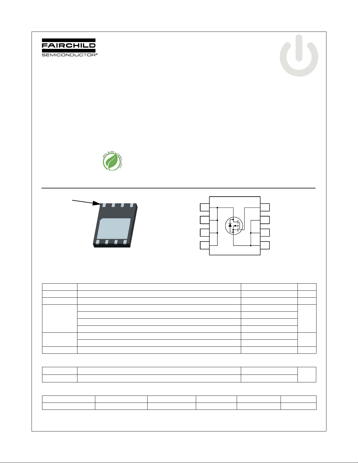
Pin 1
S
D
D
Power (Bottom view)
MOSFET Maximum Ratings T
Symbol Parameter Ratings Units
V
DS
V
GS
I
D
P
D
, T
T
J
STG
Drain to Source Voltage 100 V
Gate to Source Voltage ±20 V
Drain Current -Continuous (Package limited) TC = 25°C 22
-Continuous (Silicon limited) T
-Continuous T
-Pulsed 30
Power Dissipation TC = 25°C 78
Power Dissipation T
Operating and Storage Junction Temperature Range -55 to +150 °C
S
S
G
D
5
D
6
7
D
D
D
D
= 25°C unless otherwise noted
A
C
A
8
= 25°C 41
= 25°C (Note 1a) 7.4
A
= 25°C (Note 1a) 2.5
G
4
S
3
S
2
S
1
Thermal Characteristics
A
W
R
θJC
R
θJA
Thermal Resistance, Junction to Case 1.6
Thermal Resistance, Junction to Ambient (Note 1a) 50
Package Marking and Ordering Information
Device Marking Device Package Reel Size Tape Width Quantity
FDMS3672 FDMS3672 Power 56 13’’ 12mm 3000 units
©2007 Fairchild Semiconductor Corporation
FDMS3672 Rev.C
°C/W
1
www.fairchildsemi.com

FDMS3672 N-Channel UltraFET Trench MOSFET
Electrical Characteristics T
= 25°C unless otherwise noted
J
Symbol Parameter Test Conditions Min Typ Max Units
Off Characteristics
BV
DSS
∆BV
DSS
∆T
J
I
DSS
I
GSS
On Characteristics
V
GS(th)
∆V
GS(th)
∆T
J
r
DS(on)
g
FS
Drain to Source Breakdown Voltage ID = 250µA, VGS = 0V 100 V
Breakdown Voltage Temperature
Coefficient
Zero Gate Voltage Drain Current
Gate to Source Leakage Current VGS = ±20V, V
ID = 250µA, referenced to 25°C 104 mV/°C
VDS = 80V, 1
V
= 0V TJ = 55°C 10
GS
= 0V ±100 nA
DS
Gate to Source Threshold Voltage VGS = VDS, ID = 250µA 2 3.1 4 V
Gate to Source Threshold Voltage
Temperature Coefficient
Drain to Source On Resistance
Forward Transconductance VDS = 10V, ID = 7.4A 20 S
ID = 250µA, referenced to 25°C -11 mV/°C
VGS = 10V, ID = 7.4A 19 23
VGS = 10V, ID = 7.4A, TJ = 125°C 33 40
Dynamic Characteristics
C
iss
C
oss
C
rss
R
g
Input Capacitance
Output Capacitance 210 280 pF
Reverse Transfer Capacitance 90 135 pF
VDS = 50V, VGS = 0V,
f = 1MHz
2015 2680 pF
Gate Resistance f = 1MHz 1.3 Ω
µA
mΩVGS = 6V, ID = 6.6A 24 29
Switching Characteristics
t
d(on)
t
r
t
d(off)
t
f
Q
Q
Q
Q
g
g
gs
gd
Turn-On Delay Time
Rise Time 11 20 ns
Turn-Off Delay Time 36 58 ns
VDD = 50V, ID = 7.4A
VGS = 10V, R
GEN
Fall Time 8 16 ns
Total Gate Charge at 10V V
Total Gate Charge at 4.5V V
= 0V to 10V
GS
= 0V to 4.5V nC
GS
Gate to Source Gate Charge 9.5 nC
Gate to Drain “Miller” Charge 8 nC
Drain-Source Diode Characteristics
V
SD
t
rr
Q
rr
Notes:
1: R
θJA
the user's board design.
Source to Drain Diode Forward Voltage V
Reverse Recovery Time
Reverse Recovery Charge 101 152 nC
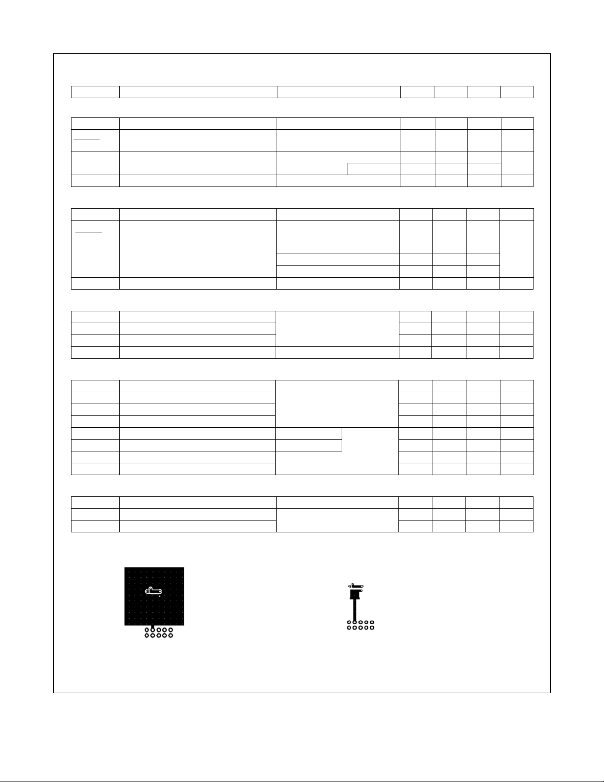
is determined with the device mounted on a 1in2 pad 2 oz copper pad on a 1.5 x 1.5 in. board of FR -4 mate rial. R
a. 50°C/W when mounted on
2
a 1 in
pad of 2 oz copper
= 0V, IS = 7.4A (Note 2) 0.8 1.2 V
GS
IF = 7.4A, di/dt = 100A/µs
= 6Ω
VDD = 50V
ID = 7.4A
23 37 ns
31 44 nC
52 78 ns
is guaranteed by design while R
θJC
b. 125°C/W when mounted on a
minimum pad of 2 oz copper
is determined by
θCA
2: Pulse Test: Pulse Width < 300µs, Duty cycle < 2.0%.
FDMS3672 Rev.C
2
www.fairchildsemi.com

FDMS3672 N-Channel UltraFET Trench MOSFET
Typical Characteristics T
60
VGS = 10V
50
40
30
20
, DRAIN CURRENT (A)
D
10
I
0
0.0 0.5 1.0 1.5 2.0 2.5 3.0
VDS, DRAIN TO SOURCE VOLTA GE (V)
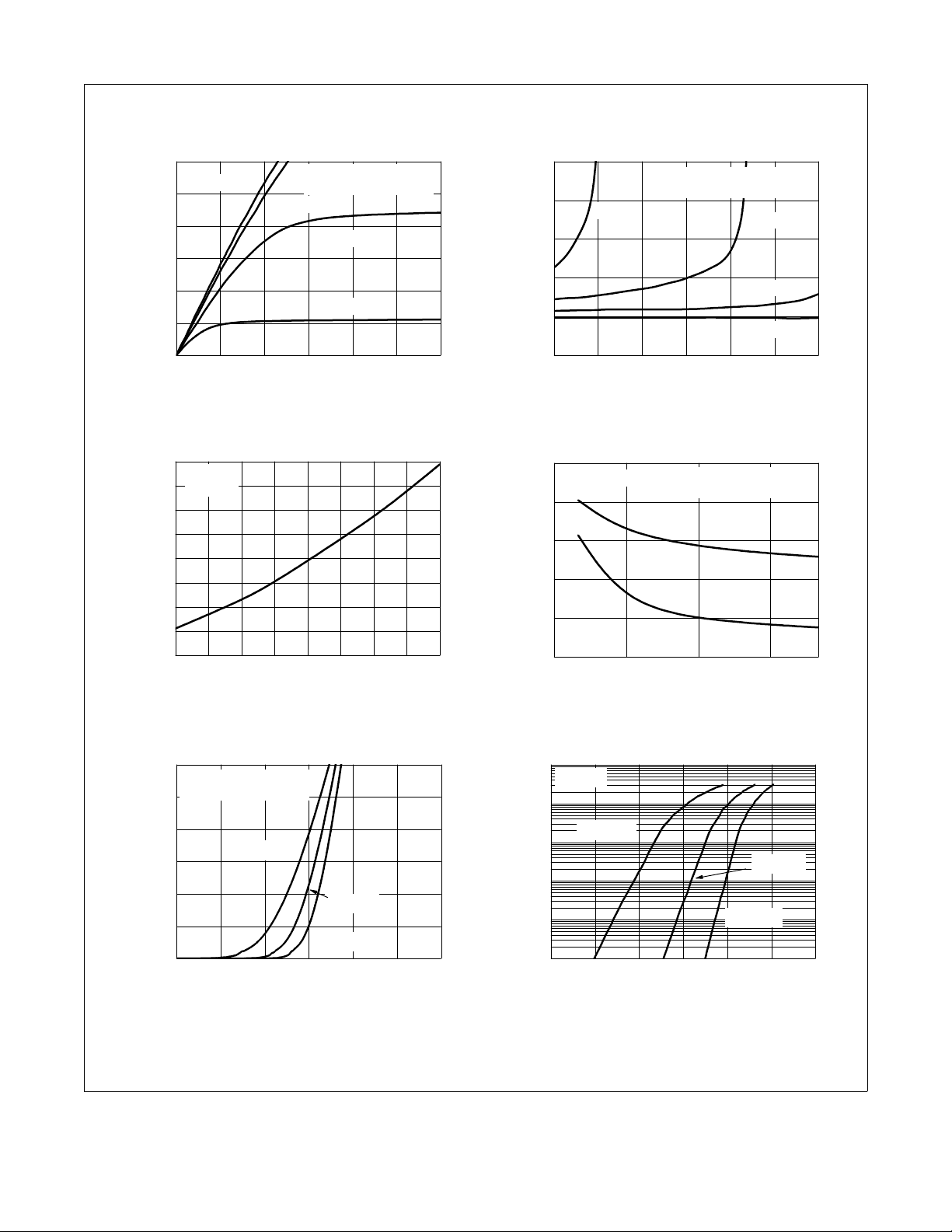
Figure 1.
2.0
1.8
On-Region Characteristics Figure 2.
ID = 7.4A
V
= 10V
GS
1.6
1.4
1.2
1.0
NORMALIZED
0.8
0.6
0.4
DRAIN TO SOURCE ON-RESISTANCE
-50 -25 0 25 50 75 100 125 150
TJ, JUNCTION TEMPERATURE (oC)
Figur e 3 . Norm al ized O n- Resis ta nce
vs Junction Temperature
PULSE DURATION = 80µs
DUTY CYCLE = 0.5%MAX
VGS = 8V
VGS = 6V
VGS = 5V
= 25°C unless otherwise noted
J
3.0
PULSE DURATION = 80µs
2.5
VGS = 5V
DUTY CYCLE = 0.5%MAX
VGS = 6V
2.0
1.5
NORMALIZED
1.0
DRAIN TO SOURCE ON-RESISTANCE
0.5
0 102030405060
ID, DRAIN CURRENT(A)
V
GS
V
Nor ma liz ed On- Res is tan ce
vs Drain Current and Gate Voltage
60
ID = 7.4A
50
(mΩ)
40
30
, DRAIN TO
DS(on)
r
20
SOURCE ON-RESISTANCE
10
4.5 6.0 7.5 9.0
VGS, GATE TO SOURCE VOLTAGE (V)
Figure 4.
On-Resistance vs Gate to
PULSE DURATION = 80µs
DUTY CYCLE = 0.5%MAX
TJ = 150oC
o
T
= 25
C
J
Source Voltage
GS
= 8V
= 10V
10
30
25
20
15
10
, DRAIN CURRENT (A)
D
I
FDMS3672 Rev.C
PULSE DURATION = 80µs
DUTY CYCLE = 0.5%MAX
TJ = 150oC
TJ = 25oC
5
TJ = -55oC
0
2345678
VGS, GATE TO SOURCE VOLTA G E (V)
Figure 5. Transfer Characteristics
100
V
= 0V
GS
10
TJ = 150oC
1
0.1
0.01
, REVERSE DRAIN CURRENT (A)
S
I
1E-3
0.0 0.2 0.4 0.6 0.8 1.0 1.2
VSD, BODY DIODE FORWA RD VO LT AGE (V)
Figure 6.
Source to Drain Diode
TJ = 25oC
TJ = -55oC
Forward Voltage vs Source Current
3
www.fairchildsemi.com
 Loading...