

Fairchild FDMS3660S service manual
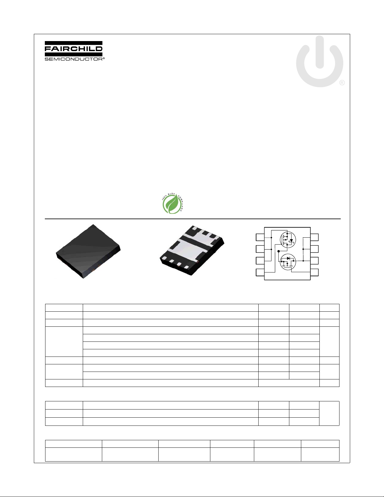
FDMS3660S
Q
Q
Power 56
G1
D1
D1
D1
G2
S2
S2
S2
D1
PHASE
(S1/D2)
S2
S2
S2
G2
D1
D1
D1
G1
Top Bottom
PHASE
PowerTrench® Power Stage
Asymmetric Dual N-Channel MOSFET
Features
Q1: N-Channel
Max r
Max r
Q2: N-Channel
Max r
Max r
Low inductance packaging shortens rise/fall times, resulting in
lower switching losses
MOSFET integration enables optimum layout for lower circuit
inductance and reduced switch node ringing
RoHS Compliant
= 8 mΩ at VGS = 10 V, ID = 13 A
DS(on)
= 11 mΩ at VGS = 4.5 V, ID = 11 A
DS(on)
= 1.8 mΩ at VGS = 10 V, ID = 30 A
DS(on)
= 2.2 mΩ at VGS = 4.5 V, ID = 27 A
DS(on)
General Description
This device includes two specialized N-Channel MOSFETs in a
dual PQFN package. The switch node has been internally
connected to enable easy placement and routing of synchronous
buck converters. The control MOSFET (Q1) and synchronous
SyncFET (Q2) have been designed to provide optimal power
efficiency.
Applications
Computing
Communications
General Purpose Point of Load
Notebook VCORE
January 2012
FDMS3660S PowerTrench
®
Power Stage
2
5
6
7
8
MOSFET Maximum Ratings T
Symbol Parameter Q1 Q2 Units
V
DS
V
GS
I
D
E
AS
P
D
TJ, T
STG
Drain to Source Voltage 30 30 V
Gate to Source Voltage (Note 3) ±20 ±12 V
Drain Current -Continuous (Package limited) TC = 25 °C 30 60
-Continuous (Silicon limited) T
-Continuous T
-Pulsed 40 120
Single Pulse Avalanche Energy 33
Power Dissipation for Single Operation TA = 25 °C 2.2
Power Dissipation for Single Operation T
Operating and Storage Junction Temperature Range -55 to +150 °C
= 25 °C unless otherwise noted
A
= 25 °C 60 145
C
= 25 °C 13
A
= 25 °C 1
A
1a
4
1a
1c
1
30
86
2.5
4
3
2
1
1b
5
1b
1d
1
A
mJ
W
Thermal Characteristics
R
θJA
θJA
R
θJC
Package Marking and Ordering Information
©2011 Fairchild Semiconductor Corporation
FDMS3660S Rev.C1
Device Marking Device Package Reel Size Tape Width Quantity
Thermal Resistance, Junction to Ambient 57
Thermal Resistance, Junction to Ambient 125
Thermal Resistance, Junction to Case 2.9 2.2
22CF
07OD
FDMS3660S Power 56 13 ” 12 mm 3000 units
1
1a
1c
1b
50
1d
120
°C/WR
www.fairchildsemi.com
FDMS3660S PowerTrench
Electrical Characteristics T
= 25 °C unless otherwise noted
J
Symbol Parameter Test Conditions Type Min Typ Max Units
Off Characteristics
BV
ΔBV
ΔT
I
DSS
I
GSS
DSS
DSS
J
= 250 μA, VGS = 0 V
Drain to Source Breakdown Voltage
Breakdown Voltage Temperature
Coefficient
D
I
= 1 mA, VGS = 0 V
D
ID = 250 μA, referenced to 25 °C
I
= 10 mA, referenced to 25 °C
D
Zero Gate Voltage Drain Current VDS = 24 V, V
V
= 20 V, VDS= 0 V
Gate to Source Leakage Current
GS
V
= 12 V, VDS= 0 V
GS
GS
= 0 V
Q1Q230
30
Q1
Q2
Q1
Q2
Q1
Q2
V
16
24
500
100
100
mV/°C
1
I
On Characteristics
V
V
GS(th)
ΔV
ΔT
r
DS(on)
g
FS
GS(th)
J
Gate to Source Threshold Voltage
Gate to Source Threshold Voltage
Temperature Coefficient
Drain to Source On Resistance
Forward Transconductance
= VDS, ID = 250 μA
GS
V
= VDS, ID = 1 mA
GS
ID = 250 μA, referenced to 25 °C
I
= 10 mA, referenced to 25 °C
D
= 10 V, ID = 13 A
V
GS
V
= 4.5 V, ID = 11 A
GS
V
= 10 V , ID = 13 A , TJ = 125 °C
GS
V
= 10 V, ID = 30 A
GS
V
= 4.5 V, ID = 27 A
GS
V
= 10 V , ID = 30 A , TJ = 125 °C
GS
V
= 5 V, ID = 13 A
DS
V
= 5 V, ID = 30 A
DS
Q1Q21.1
1.1
Q1
Q2
Q1
Q2
Q1
Q2
1.9
1.5
-6
-3
4
6
5.7
1.3
1.5
1.86
62
231
2.7
2.2
mV/°C
8
11
8.7
1.8
2.2
2.6
μA
μA
nA
nA
V
mΩ
S
®
Power Stage
Dynamic Characteristics
C
iss
C
oss
C
rss
R
g
Input Capacitance
Output Capacitance
Reverse Transfer Capacitance
Gate Resistance
Switching Characteristics
t
d(on)
t
r
t
d(off)
t
f
Q
Q
Q
Q
g
g
gs
gd
Turn-On Delay Time
Rise Time
Turn-Off Delay Time
Fall Time
Total Gate Charge V
Total Gate Charge V
Gate to Source Gate Charge
Gate to Drain “Miller” Charge
1325
Q1:
= 15 V, VGS = 0 V, f = 1 MHZ
V
DS
Q2:
= 15 V, VGS = 0 V, f = 1 MHZ
V
DS
Q1
Q2
Q1
Q2
Q1
Q2
Q1Q20.2
0.2
1765
4130
5493
466
620
915
1220
46
12470185
0.6
0.8
pF
pF
pF
2
3
Ω
7.71115
20
2.2510
10
19
40
34
64
1.8
3.91010
21
62
29
87
9.52913
41
3.9
9
2.6
7
ns
ns
ns
ns
nC
nC
nC
nC
Q1:
= 15 V, ID = 13 A, R
V
DD
Q2:
= 15 V, ID = 30 A, R
V
DD
= 0 V to 10 V
GS
= 0 V to 4.5 V
GS
= 6 Ω
GEN
= 6 Ω
GEN
Q1:
V
= 15 V,
DD
I
= 13 A
D
Q2:
VDD = 15 V,
I
= 30 A
D
Q1
Q2
Q1
Q2
Q1
Q2
Q1
Q2
Q1
Q2
Q1
Q2
Q1
Q2
Q1
Q2
©2011 Fairchild Semiconductor Corporation
FDMS3660S Rev.C1
2
www.fairchildsemi.com
FDMS3660S PowerTrench
Electrical Characteristics T
= 25 °C unless otherwise noted
J
Symbol Parameter Test Conditions Type Min Typ Max Units
Drain-Source Diode Characteristics
1.2
V
= 0 V, IS = 13 A (Note 2)
GS
V
= 0 V, IS = 2 A (Note 2)
V
SD
t
rr
Q
rr
Notes:
1: R
θJA
by the user's board design.
Source to Drain Diode Forward Voltage
Reverse Recovery Time
Reverse Recovery Charge
is determined with the device mounted on a 1 in2 pad 2 oz copper pad on a 1.5 x 1.5 in. board of FR-4 material. R
a. 57 °C/W when mounted on
2
a 1 in
pad of 2 oz copper
c. 125 °C/W when mounted on a
minimum pad of 2 oz copper
GS
V
= 0 V, IS = 30 A (Note 2)
GS
V
= 0 V, IS = 2 A (Note 2)
GS
Q1:
I
= 13 A, di/dt = 100 A/μs
F
Q2:
I
= 30 A, di/dt = 300 A/μs
F
Q1
Q1
Q2
Q2
Q1
Q2
Q1
Q2
is guaranteed by design while R
θJC
b. 50 °C/W when mounted on
2
a 1 in
pad of 2 oz copper
d. 120 °C/W when mounted on a
minimum pad of 2 oz copper
0.8
1.2
0.7
0.8
0.6
26
29
10
32
1.2
1.2
42
46
20
50
θCA
is determined
V
ns
nC
®
Power Stage
2: Pulse Test: Pulse Width < 300 μs, Duty cycle < 2.0%.
3: As an N-ch device, the negative Vgs rating is for low duty cycle pulse ocurrence only. No continuous rating is implied with the negative Vgs rating.
4: EAS of 33 mJ is based on starting TJ = 25 oC; N-ch: L = 1.9 mH, IAS = 6 A, VDD = 27 V, VGS = 10 V. 100% test at L= 0.1 mH, IAS = 16 A.
5: EAS of 86 mJ is based on starting TJ = 25 oC; N-ch: L = 0.6 mH, IAS = 17 A, VDD = 27 V, VGS = 10 V. 100% test at L= 0.1 mH, IAS = 31 A.
©2011 Fairchild Semiconductor Corporation
FDMS3660S Rev.C1
3
www.fairchildsemi.com
FDMS3660S PowerTrench
0.0 0.2 0.4 0.6 0.8 1.0
0
10
20
30
40
V
GS
= 6 V
V
GS
= 4 V
V
GS
= 10 V
V
GS
= 4.5 V
V
GS
= 3.5 V
PULSE DURATION = 80 μs
DUTY CYCLE = 0.5% MAX
I
D
, DRAIN CURRENT (A)
V
DS
, DRAIN TO SOURCE VOLTAGE (V)
0 10203040
0
1
2
3
4
VGS = 6 V
VGS = 3.5 V
PULSE DURA TION = 80 μs
DUTY CYCLE = 0.5% MAX
NORMALIZED
DRAIN TO SOURCE ON-RESISTA NCE
I
D
, DRAIN CURRENT (A)
V
GS
= 4 V
VGS = 4.5 V
V
GS
= 10 V
-75 -50 -25 0 25 50 75 100 125 150
0.6
0.8
1.0
1.2
1.4
1.6
ID = 13 A
V
GS
= 10 V
NORMALIZED
DRAIN TO SOURCE ON-RESISTANCE
T
J
, JUNCTION TEMPERATURE (
o
C)
246810
0
4
8
12
16
20
TJ = 125 oC
ID = 13 A
TJ = 25 oC
V
GS
, GATE TO SOURCE VOLTA GE (V)
r
DS(on)
,
DRAIN TO
SOURCE ON-RESISTANCE
(mΩ)
PULSE DURA TION = 80 μs
DUTY CYCLE = 0.5% MAX
1.5 2.0 2.5 3.0 3.5 4.0
0
10
20
30
40
TJ = 150 oC
V
DS
= 5 V
PULSE DURA TION = 80 μs
DUTY CYCLE = 0.5% MAX
TJ = -55 oC
TJ = 25 oC
I
D
, DRAIN CURRENT (A)
VGS, GATE TO SOURCE VOLTAGE (V)
0.0 0.2 0.4 0.6 0.8 1.0 1.2
0.001
0.01
0.1
1
10
40
TJ = -55 oC
TJ = 25 oC
TJ = 150 oC
V
GS
= 0 V
I
S
, REVERSE DRAIN CURRENT (A)
VSD, BODY DIODE FORWARD VOLTAGE (V)
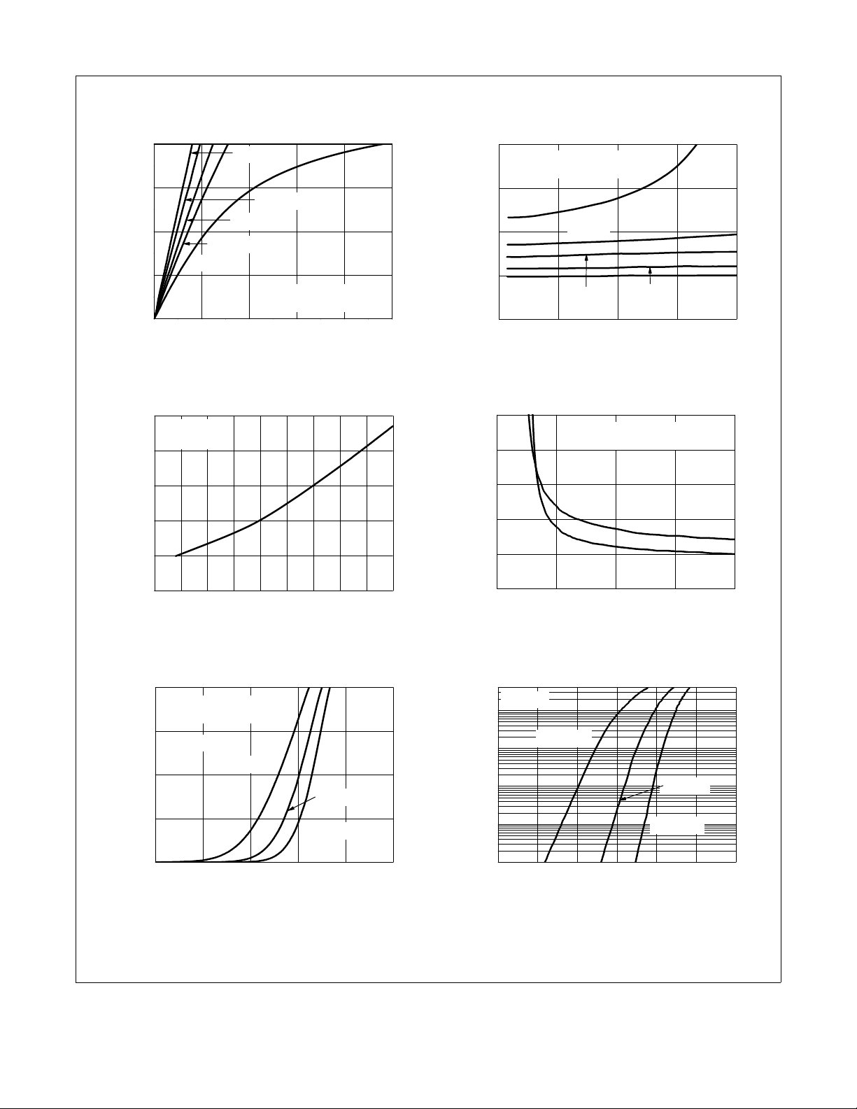
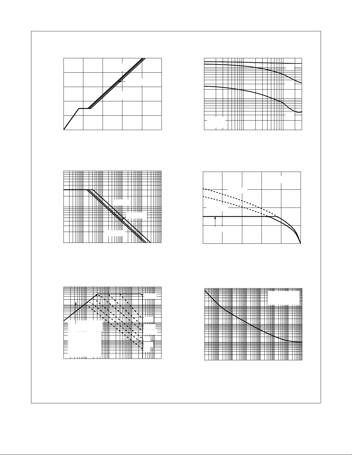
Typical Characteristics (Q1 N-Channel) T
Figure 1.
On Region Characteristics Figure 2.
= 25 °C unless otherwise noted
J
Norm a l i z e d O n - R e sistance
vs Drain Current and Gate Voltage
®
Power Stage
Fi g u r e 3. No r m alized O n Resist a n ce
vs Junction Temperature
©2011 Fairchild Semiconductor Corporation
FDMS3660S Rev.C1
Figure 5. Transfer Characteristics
Figure 4.
On-Res istance vs Gate to
Source Voltage
Figure 6.
Source to Drain Diode
Forward Voltage vs Source Current
4
www.fairchildsemi.com
FDMS3660S PowerTrench
0 5 10 15 20 25
0
2
4
6
8
10
ID = 13 A
V
DD
= 20 V
V
DD
= 10 V
V
GS
, GATE TO SOURCE VOLTAGE (V)
Qg, GATE CHARGE (nC)
VDD = 15 V
0.1 1 10 30
10
100
1000
2000
f = 1 MH z
V
GS
= 0 V
CAPACITANCE (pF)
VDS, DRAIN TO SOURCE VOL T AGE (V)
C
rss
C
oss
C
iss
0.001 0.01 0.1 1 10 100
1
10
100
TJ = 100 oC
TJ = 25 oC
TJ = 125 oC
tAV, TIME IN AVALANCHE (ms)
I
AS
, AVALANCHE CURRENT (A)
25 50 75 100 125 150
0
20
40
60
80
R
θJC
= 2.9 oC/W
V
GS
= 4.5 V
Limited by Package
V
GS
= 10 V
I
D
, DRAIN CURRENT (A)
T
C
, CASE TEMPERATURE (
o
C)
0.01 0.1 1 10 100200
0.01
0.1
1
10
100
100 μs
DC
100 ms
10 ms
1 ms
1 s
I
D
, DRAIN CURRENT (A)
VDS, DRAIN to SOURCE VOLTAGE (V)
THIS A REA IS
LIMITED BY r
DS(on)
SINGLE PULSE
T
J
= MAX RATED
R
θJA
= 125
o
C/W
T
A
= 25
o
C
10 s
10-410-310-210
-1
110
100 1000
0.1
1
10
100
1000
SINGLE PULSE
R
θJA
= 125 oC/W
P(
PK
), PEAK TRANSIENT POWER (W)
t, PULSE WIDTH (sec)
Typical Characteristics (Q1 N-Channel) T
Figure 7.
Gate Charge Characteristics Figure 8.
= 25 °C unless otherwise noted
J
Capa c i t a nce v s D r ain
to Source Voltage
®
Power Stage
Figure 9.
Un c l a mp e d I nd u c tiv e
Switching Capability
©2011 Fairchild Semiconductor Corporation
FDMS3660S Rev.C1
Figure 11. Forward Bias Safe
Op
erating Area
Figure 10.
Maximum Continuous Drain
Current vs Case Temperature
Figure 12. Single Pulse Maximum
Power Dissipation
5
www.fairchildsemi.com
 Loading...