Fairchild FDMS2672 service manual

April 2012
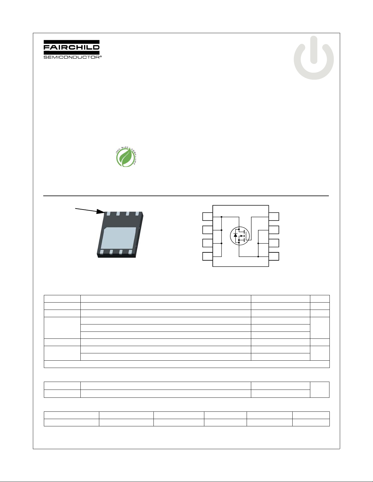
FDMS2672 N-Channel UltraFET Trench MOSFET
FDMS2672
N-Channel UltraFET Trench MOSFET
200V, 20A, 77m:
Features
Max r
Max r
Low Miller Charge
RoHS Compliant
= 77m: at VGS = 10V, ID = 3.7A
DS(on)
= 88m: at VGS = 6V, ID = 3.5A
DS(on)
Pin 1
S
S
S
G
General Description
UItraFET devices combine characteristics that enable
benchmark efficiency in power conversion applications.
Optimized for r
these devices are ideal for high frequency DC to DC converters.
DS(on)
Application
DC - DC Conversion
D
5
D
6
7
D
, low ESR, low total and Miller gate charge,
G
4
S
3
S
2
tm
D
D
D
Power 56 (Bottom view)
MOSFET Maximum Ratings T
Symbol Parameter Ratings Units
V
DS
V
GS
I
D
E
AS
P
D
, T
T
J
STG
Drain to Source Voltage 200 V
Gate to Source Voltage ±20 V
Drain Current -Continuous (Silicon limited) TC = 25°C 20
-Pulsed 20
Single Pulse Avalanche Energy (Note 3) 33.8 mJ
Power Dissipation TC = 25°C 78
Power Dissipation T
Operating and Storage Junction Temperature Range -55 to +150 °C
D
D
= 25°C unless otherwise noted
A
8
= 25°C (Note 1a) 3.7
A
= 25°C (Note 1a) 2.5
A
S
1
Thermal Characteristics
R
TJC
R
TJA
Thermal Resistance, Junction to Case 1.6
Thermal Resistance, Junction to Ambient (Note 1a) 50
Package Marking and Ordering Information
Device Marking Device Package Reel Size Tape Width Quantity
FDMS2672 FDMS2672 Power 56 13’’ 12mm 3000 units
A -Continuous T
W
°C/W
©2012 Fairchild Semiconductor Corporation
FDMS26
72 Rev.C
1
1
www.fairchildsemi.com

FDMS2672 N-Channel UltraFET Trench MOSFET
Electrical Characteristics T
= 25°C unless otherwise noted
J
Symbol Parameter Test Conditions Min Typ Max Units
Off Characteristics
BV
DSS
'BV
DSS
'T
J
I
DSS
I
GSS
On Characteristics
V
GS(th)
'V
GS(th)
'T
J
r
DS(on)
g
FS
Drain to Source Breakdown Voltage ID = 250PA, VGS = 0V 200 V
Breakdown Voltage Temperature
Coefficient
I
= 250PA, referenced to 25°C 210 mV/°C
D
Zero Gate Voltage Drain Current VDS = 160V 1 PA
Gate to Source Leakage Current VGS = ±20V, V
= 0V ±100 nA
DS
Gate to Source Threshold Voltage VGS = VDS, ID = 250PA 2 3.1 4 V
Gate to Source Threshold Voltage
Temperature Coefficient
Drain to Source On Resistance
Forward Transconductance VDS = 10V, ID = 3.7A 14 S
= 250PA, referenced to 25°C -10 mV/°C
I
D
V
= 10V, ID = 3.7A 64 77
GS
= 6V, ID = 3.5A 69 88
GS
= 10V, ID = 3.7A TJ = 125°C 129 156
V
GS
Dynamic Characteristics
C
iss
C
oss
C
rss
R
g
Input Capacitance
Output Capacitance 95 125 pF
Reverse Transfer Capacitance 30 45 pF
V
= 100V, VGS = 0V,
DS
f = 1MHz
Gate Resistance
1740 2315 pF
0.1
1
5
Switching Characteristics
t
d(on)
t
r
t
d(off)
t
f
Q
g(TOT)
Q
gs
Q
gd
Turn-On Delay Time
Rise Time 11 22 ns
Turn-Off Delay Time 36 57 ns
VDD = 100V, ID = 3.7A
V
GS
= 10V, R
GEN
= 6:
Fall Time 10 20 ns
Total Gate Charge at 10V V
Gate to Source Gate Charge 7 nC
= 0V to 10V
GS
V
DD
I
D
= 100V
= 3.7A
Gate to Drain “Miller” Charge 8 nC
22 34 ns
30 42 nC
m:V
:
Drain-Source Diode Characteristics
V
SD
t
rr
Q
rr
Notes:
1: R
TJA
the user's board design.
2: Pulse Test: Pulse Width < 300Ps, Duty cycle < 2.0%.
3: EAS of 33.8mJ is based on starting TJ = 25 C, L = 3mH, IAS = 4.75A, VDD = 25V, V
FDMS2672 Rev.C1
Source to Drain Diode Forward Voltage V
Reverse Recovery Time
Reverse Recovery Charge 238 357 nC
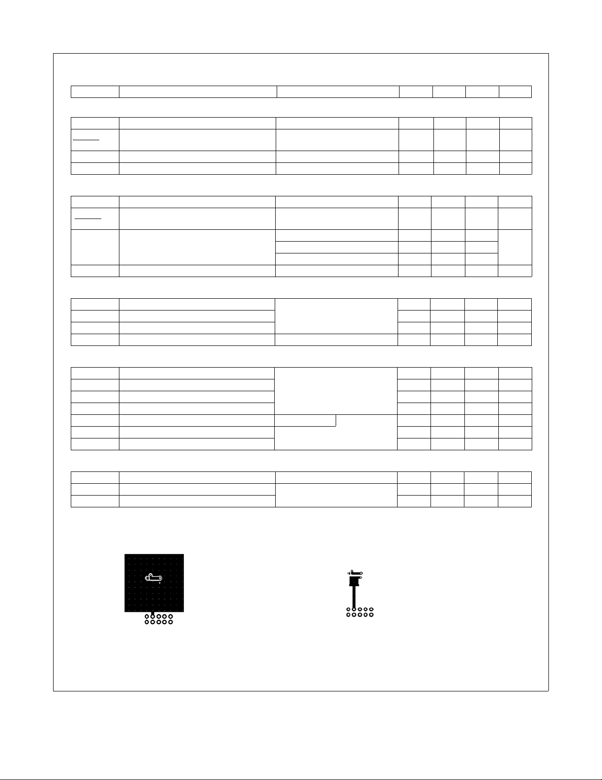
is determined with the device mounted on a 1in2 pad 2 oz copper pad on a 1.5 x 1.5 in. board of FR-4 material. R
a. 50°C/W when mounted on
2
pa d o f 2 oz co pp er
a 1 in
°
= 0V, IS = 3.7A (Note 2) 0.8 1.2 V
GS
= 3.7A, di/dt = 100A/Ps
I
F
= 10V.
GS
2
70 105 ns
is guaranteed by design while R
TJC
b. 125°C/W when mounted on a
minimum pad of 2 oz copper
is determined by
TCA
www.fairchildsemi.com

FDMS2672 N-Channel UltraFET Trench MOSFET
:
Typical Characteristics T
40
PULSE DURATION = 80Ps
DUTY CYCLE = 0.5%MAX
30
20
10
, DRAIN CURRENT (A)
D
I
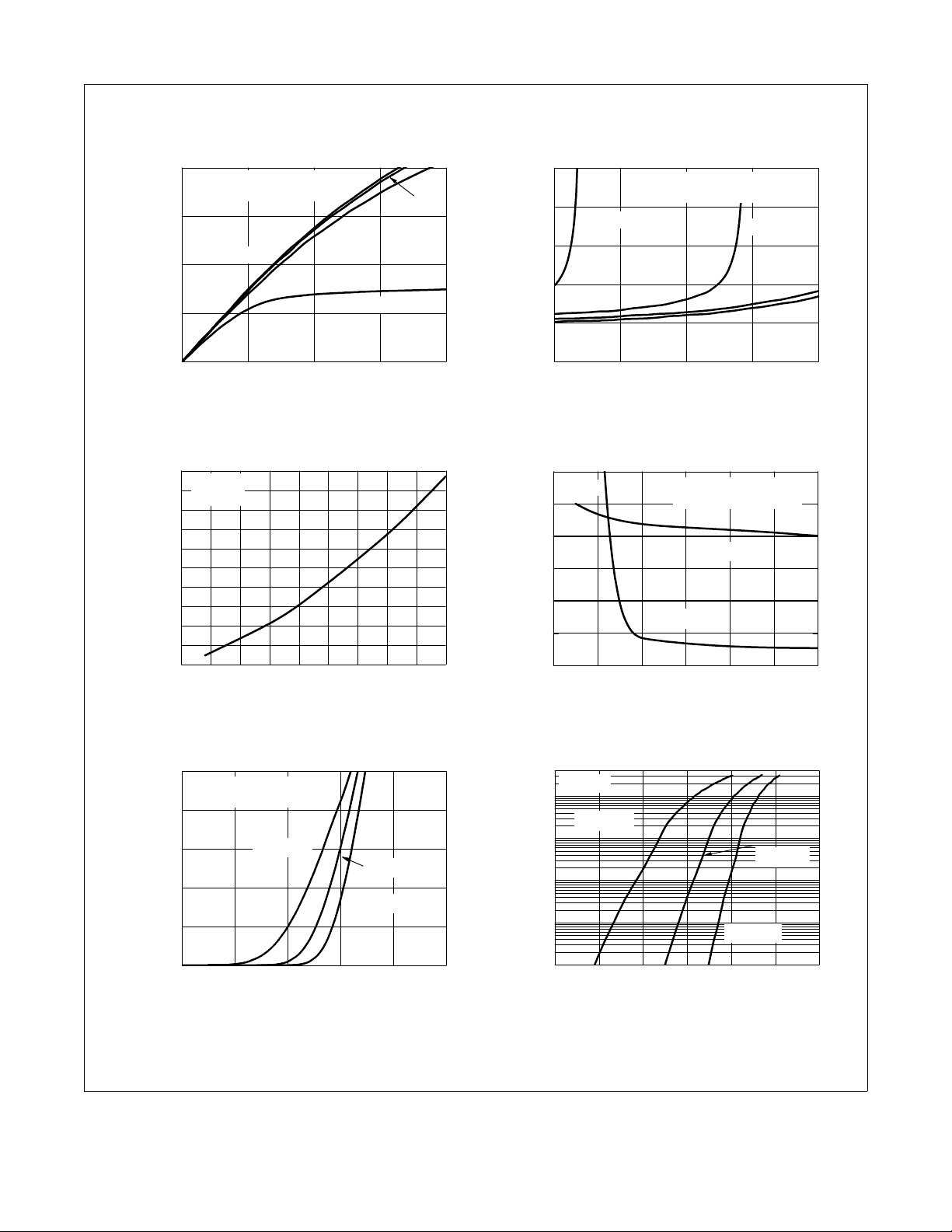
Figure 1.
2.4
2.2
2.0
1.8
1.6
1.4
1.2
1.0
NORMALIZED
0.8
0.6
0.4
DRAIN TO SOURCE ON-RESISTANCE
-75 -50 -25 0 25 50 75 100 125 150
F i g u r e 3 . N o r m a l i z e d O n R e s i s t a n c e
VGS = 10V
0
01234
VDS, DRAIN TO SOURCE VOLTAGE (V)
On Region Characteristics Figure 2.
ID = 3.7A
= 10V
V
GS
TJ, JUNCTION TEMPERATURE (oC)
vs Junction Temperature
= 25°C unless otherwise noted
J
VGS = 8V
VGS = 6V
VGS = 5V
3.0
PULSE DURATION = 80Ps
DUTY CYCLE = 0.5%MAX
2.5
VGS = 5V
VGS = 6V
2.0
1.5
NORMALIZED
1.0
DRAIN TO SOURCE ON-RESISTANCE
0.5
0 10203040
ID, DRAIN CURRENT(A)
V
= 8V
GS
V
= 10V
GS
N o r m a l i z e d O n - R e s i s t a n c e
vs Drain Current and Gate Voltage
200
)
ID = 4.5A
175
(m
150
125
, DRAIN TO
100
DS(on)
r
75
SOURCE ON-RESISTANCE
50
45678910
VGS, GATE TO SOURCE VOLTAGE (V)
Figure 4.
O n - R es i s t a n c e vs G a t e t o
PULSE DURATION = 80Ps
DUTY CYCLE = 0.5%MAX
TA = 150oC
TA = 25oC
Source Voltage
25
20
15
10
, DRAIN CURRENT (A)
D
I
FDMS2672 Rev.C1
PULSE DURATION = 80Ps
DUTY CYCLE = 0.5%MAX
TJ = 150oC
TJ = 25oC
TJ = -55oC
5
0
234567
VGS, GATE TO SOURCE VOLTAGE (V)
Figure 5. Transfer Characteristics
40
V
= 0V
GS
10
TJ = 150oC
1
TJ = 25oC
0.1
0.01
, REVERSE DRAIN CURRENT (A)
S
I
1E-3
0.0 0.2 0.4 0.6 0.8 1.0 1.2
VSD, BODY DIODE FORWARD VOLTAGE (V)
Figure 6.
S o u r ce t o D r a i n Di o d e
TJ = -55oC
Forward Voltage vs Source Current
3
www.fairchildsemi.com
 Loading...