tm
FDMS2572
N-Channel UltraFET Trench® MOSFET
150V, 27A, 47mΩ
Features
Max r
Max r
Low Miller Charge
Optimized efficiency at high frequencies
UIS Capability (Single pulse and Repetitive pulse)
RoHS Compliant
= 47mΩ at VGS = 10V, ID = 4.5A
DS(on)
= 53mΩ at VGS = 6V, ID = 4.5A
DS(on)
General Description
UItraFET devices combine characteristics that enable
benchmark efficiency in power conversion applications.
Optimized for r
these devices are ideal for high frequency DC to DC converters.
DS(on)
Application
Distributed Power Architectures and VRMs
Primary Switch for 24V and 48V Systems
High Voltage Synchronous Rectifier
FDMS2572 N-Channel UltraFET Trench
February 2007
, low ESR, low total and Miller gate charge,
®
MOSFET
Pin 1
S
D
D
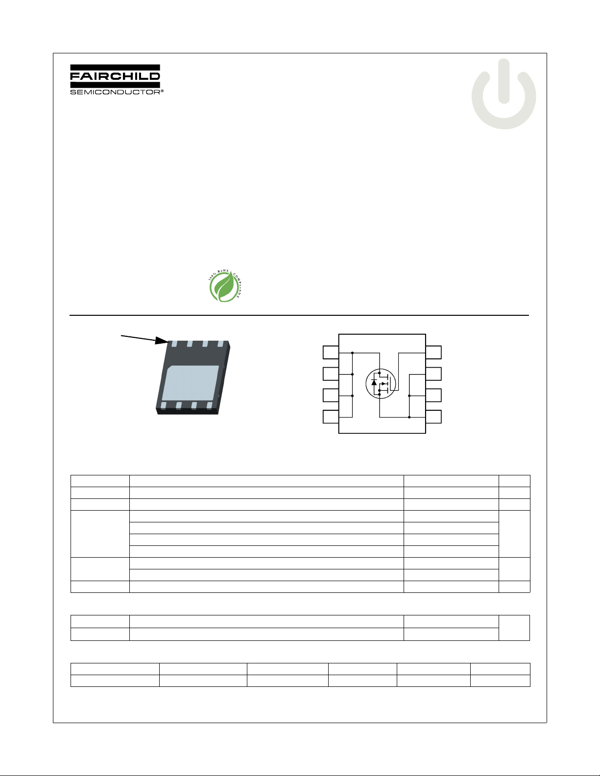
Power 56 (Bottom view)
MOSFET Maximum Ratings T
Symbol Parameter Ratings Units
V
DS
V
GS
I
D
P
D
, T
T
J
STG
Drain to Source Voltage 150 V
Gate to Source Voltage ±20 V
Drain Current -Continuous (Package limited) TC = 25°C 27
-Continuous (Silicon limited) T
-Continuous T
-Pulsed 30
Power Dissipation TC = 25°C 78
Power Dissipation T
Operating and Storage Junction Temperature Range -55 to +150 °C
S
S
G
D
5
D
6
7
D
D
D
D
= 25°C unless otherwise noted
A
8
= 25°C 27
C
= 25°C (Note 1a) 4.5
A
= 25°C (Note 1a) 2.5
A
G
4
S
3
S
2
S
1
Thermal Characteristics
A
W
R
θJC
R
θJA
Thermal Resistance, Junction to Case 1.6
Thermal Resistance, Junction to Ambient (N ote 1a) 50
Package Marking and Ordering Information
Device Marking Device Package Reel Size Tape Width Quantity
FDMS2572 FDMS2572 Power 56 13’’ 12mm 3000 units
©2007 Fairchild Semiconductor Corporation
FDMS2572 Rev.C2
°C/W
1
www.fairchildsemi.com

FDMS2572 N-Channel UltraFET Trench
Electrical Characteristics T
= 25°C unless otherwise noted
J
Symbol Parameter Test Conditions Min Typ Max Units
Off Characteristics
BV
DSS
∆BV
DSS
∆T
J
I
DSS
I
GSS
On Characteristics
V
GS(th)
∆V
GS(th)
∆T
J
r
DS(on)
g
FS
Drain to Source Breakdown Voltage ID = 250µA, VGS = 0V 150 V
Breakdown Voltage Temperature
Coefficient
Zero Gate Voltage Drain Current VDS = 120V, V
Gate to Source Leakage Current VGS = ±20V, V
ID = 250µA, referenced to 25°C 180 mV/°C
= 0V 1 µA
GS
= 0V ±100 nA
DS
(Note 2)
Gate to Source Threshold Voltage VGS = VDS, ID = 250µA 2 3 4 V
Gate to Source Threshold Voltage
Temperature Coefficient
Drain to Source On Resistance
Forward Transconductance VDS = 10V, ID = 4.5A 14 S
ID = 250µA, referenced to 25°C -9.8 mV/°C
VGS = 10V, ID = 4.5A 36 47
VGS = 10V, ID = 4.5A, TJ = 125°C 69 103
Dynamic Characteristics
C
iss
C
oss
C
rss
R
g
Input Capacitance
Output Capacitance 130 175 pF
Reverse Transfer Capacitance 30 45 pF
VDS = 75V, VGS = 0V,
f = 1MHz
1960 2610 pF
Gate Resistance f = 1MHz 1.3 Ω
Switching Characteristics
t
d(on)
t
r
t
d(off)
t
f
Q
g(TOT)
Q
gs
Q
gd
Turn-On Delay Time
Rise Time 8 16 ns
Turn-Off Delay Time 38 61 ns
VDD = 75V, ID = 1.0A
VGS = 10V, R
GEN
= 6Ω
11 20 ns
Fall Time 31 50 ns
Total Gate Charge at 10V V
Gate to Source Gate Charge 9 nC
= 0V to 10V
GS
VDD = 75V
ID = 4.5A
31 43 nC
Gate to Drain “Miller” Charge 7 nC
mΩVGS = 6V, ID = 4.5A 39 53
®
MOSFET
Drain-Source Diode Characteristics
V
SD
t
rr
Q
rr
Notes:
1: R
θJA
the user's board design.
2: Pulse Test: Pulse Width < 300µs, Duty cycle < 2.0%.
FDMS2572 Rev.C2
Source to Drain Diode Forward Voltage V
Reverse Recovery Time
Reverse Recovery Charge 130 195 nC
is determined with the device mounted on a 1in2 pad 2 oz copper pad on a 1.5 x 1.5 in. board of FR-4 material. R
IF = 4.5A, di/dt = 100A/µs
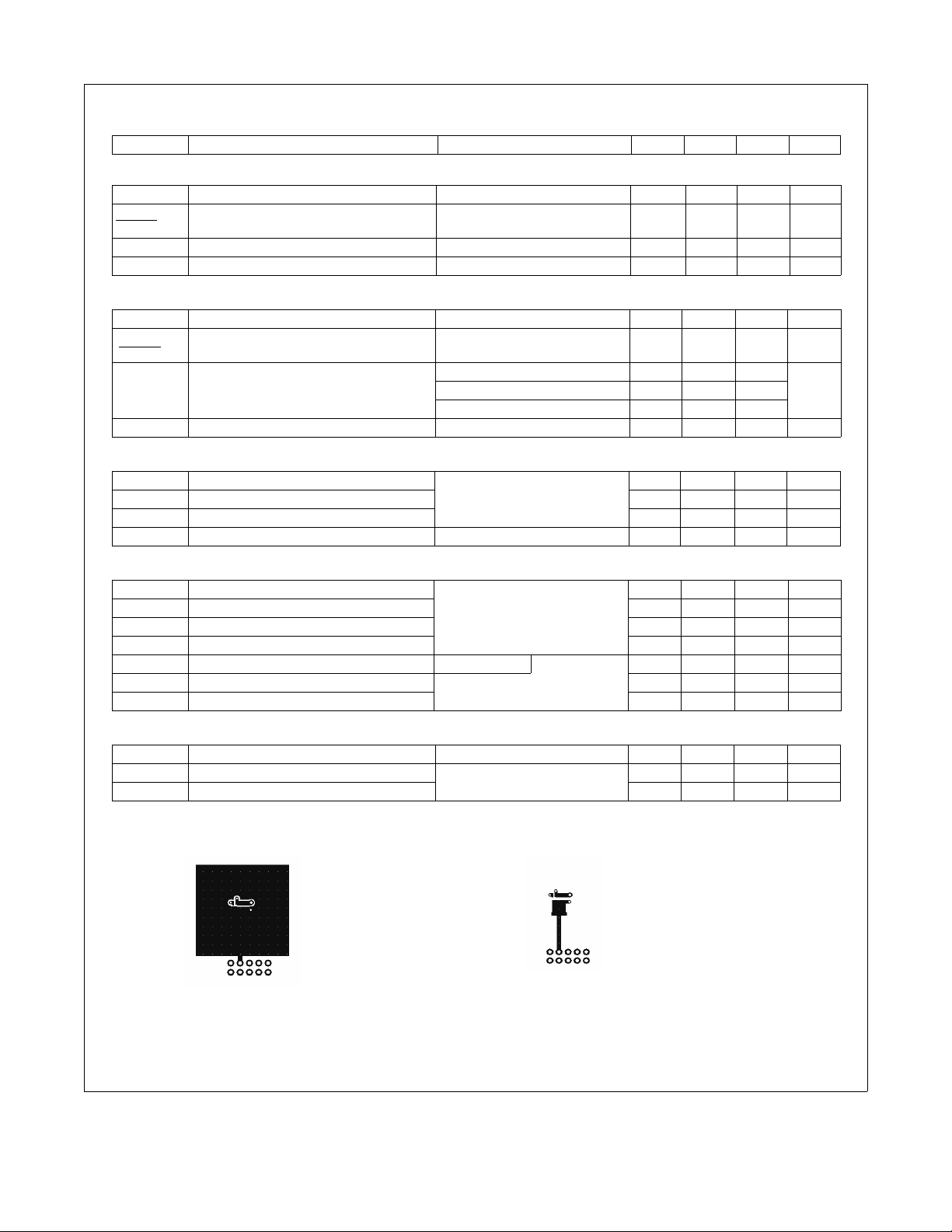
a.50°C/W when mounted on
a 1 in2 pad of 2 oz copper
= 0V, IS = 2.2A (Note 2) 0.7 1.0 V
GS
67 101 ns
is guaranteed by design while R
θJC
b. 125°C/W when mounted on a
minimum pad of 2 oz copper
2
is determined by
θCA
www.fairchildsemi.com

FDMS2572 N-Channel UltraFET Trench
Typical Characteristics T
40
VGS = 10V
35
VGS = 6V
30
25
20
15
10
, DRAIN CURRENT (A)
D
I
5
0
012345
VDS, DRAIN TO SOURCE VOLTAGE (V)
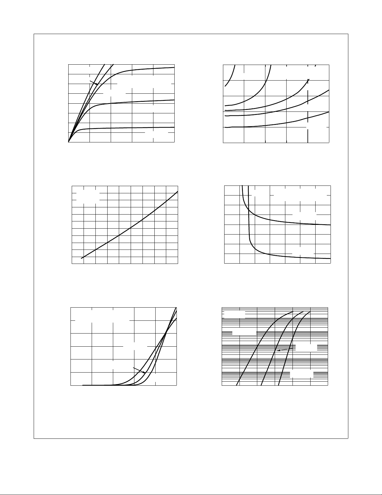
Figure 1.
2.4
2.2
2.0
1.8
1.6
1.4
1.2
1.0
NORMALIZED
0.8
0.6
0.4
0.2
DRAIN TO SOURCE ON-RESISTANCE
-75 -50 -25 0 25 50 75 100 125 150
On-Region Characteristics Figure 2.
ID = 4.5A
V
= 10V
GS
TJ, JUNCTION TEMPERATURE (oC)
F i g u r e 3 . N o r m a l i z e d O n - R e s i s t a n c e
vs Junction Temperature
60
PULSE DURATION = 300µs
DUTY CYCLE = 2.0 %MAX
50
PULSE DURATION = 300µs
DUTY CYCLE = 2.0%MAX
VGS = 5.5V
= 25°C unless otherwise noted
J
VGS = 5V
VGS = 4.5V
1.8
VGS =4.5V
0 8 16 24 32 40
ID, DRAIN CURRENT(A)
NORMALIZED
1.6
1.4
1.2
1.0
0.8
DRAIN TO SOURCE ON-RESISTANCE
PULSE DURATION = 300µs
DUTY CYCLE = 2.0%MAX
VGS =5V
N o r m a l i z e d O n - R e s i s t a n c e
vs Drain Current and Gate Voltage
110
PULSE DURATION =300µs
DUTY CYCLE = 2.0%MAX
, DRAIN TO
DS(on)
r
100
90
(mOHM)
80
70
60
50
40
30
SOURCE ON-RESISTANCE
345678910
Figure 4.
ID = 4.5A
VGS, GATE TO SOURCE VOLTAGE (V)
O n - R es i s t a n c e vs G a t e t o
Source Voltage
60
V
= 0V
GS
10
VGS =5.5V
VGS = 6V
VGS = 10V
TJ = 150oC
o
T
= 25
J
®
MOSFET
C
40
30
20
, DRAIN CURRENT (A)
10
D
I
0
FDMS2572 Rev.C2
TJ = 125oC
TJ = 25oC
TJ =-55oC
123456
VGS, GATE TO SOURCE VOLTAGE (V)
Figure 5. Transfer Characteristics
3
1
TJ = 125oC
0.1
0.01
1E-3
, REVERSE DRAIN CURRENT (A)
S
I
1E-4
0.0 0.2 0.4 0.6 0.8 1.0 1.2
VSD, BODY DIODE FORWARD VOLTAGE (V)
Figure 6.
S o u r ce t o D r a i n Di o d e
TJ = 25oC
TJ = -55oC
Forward Voltage vs Source Current
www.fairchildsemi.com
 Loading...