


FDMS2510SDC
4
3
2
1
5
6
7
8
S
S
S
G
D
D
D
D
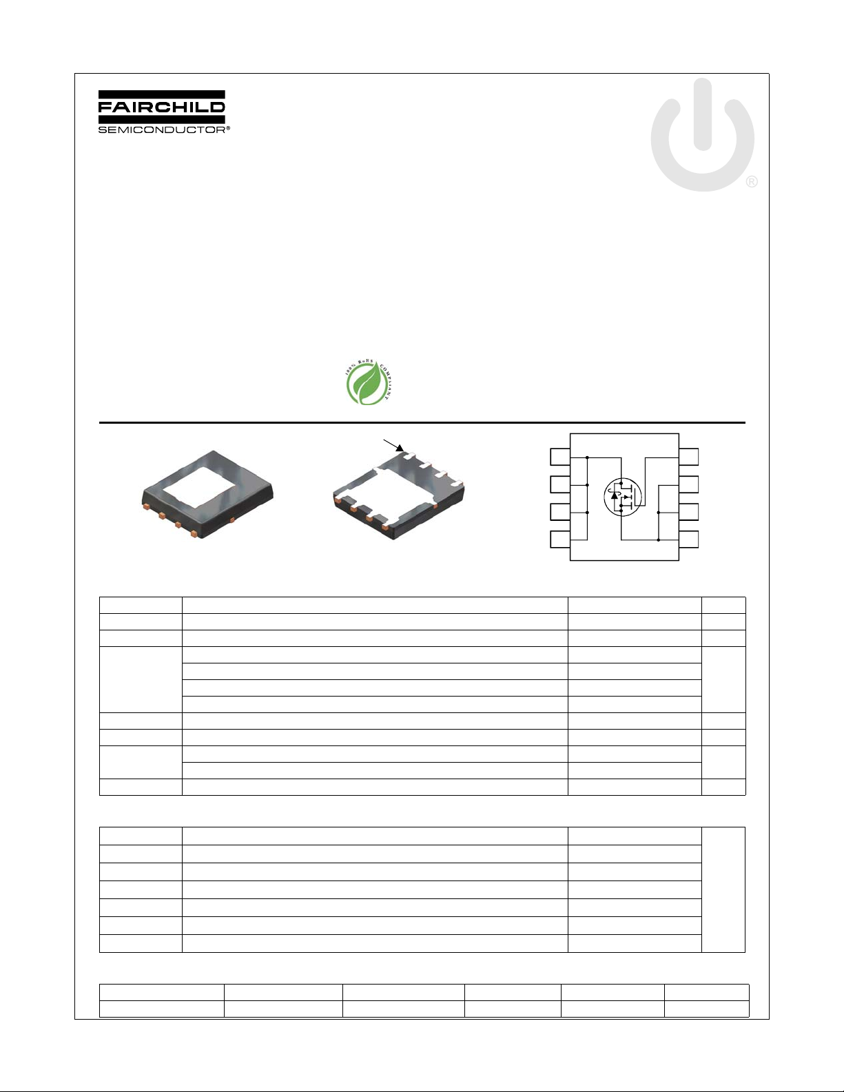
Bottom Top
Pin 1
D
D
D
D
G
S
S
S
Power 56
N-Channel Dual CoolTM PowerTrench® SyncFET
25 V, 49 A, 2.9 mΩ
Features
Dual CoolTM Top Side Cooling PQFN package
Max r
Max r
High performance technology for extremely low r
SyncFET Schottky Body Diode
RoHS Compliant
= 2.9 mΩ at VGS = 10 V, ID = 23 A
DS(on)
= 4.2 mΩ at VGS = 4.5 V, ID = 18 A
DS(on)
DS(on)
General Description
This N-Channel MOSFET is produced using Fairchild
Semiconductor’s advanced PowerTrench
Advancements in both silicon and Dual Cool
technologies have been combined to offer the lowest r
while maintaining excellent switching performance by extremely
low Junction-to-Ambient thermal resistance. This device has the
added benefit of an efficient monolithic Schottky body diode.
Applications
Synchronous Rectifier for DC/DC Converters
Telecom Secondary Side Rectification
High End Server/Workstation Vcore Low Side
TM
July 2010
®
process.
TM
package
DS(on)
FDMS2510SDC N-Channel Dual Cool
TM
PowerTrench
®
SyncFET
MOSFET Maximum Ratings T
Symbol Parameter Ratings Units
V
DS
V
GS
I
D
E
AS
dv/dt Peak Diode Recovery dv/dt (Note 5) 2.5 V/ns
P
D
, T
T
J
STG
Drain to Source Voltage 25 V
Gate to Source Voltage (Note 4) ±20 V
Drain Current -Continuous (Package limited) TC = 25 °C 49
-Continuous (Silicon limited) T
-Continuous T
-Pulsed 200
Single Pulse Avalanche Energy (Note 3) 84 mJ
Power Dissipation TC = 25 °C 60
Power Dissipation T
Operating and Storage Junction Temperature Range -55 to +150 °C
= 25°C unless otherwise noted
A
= 25 °C 117
C
= 25 °C (Note 1a) 28
A
= 25 °C (Note 1a) 3.3
A
A
W
Thermal Characteristics
R
θJC
R
θJC
R
θJA
R
θJA
R
θJA
R
θJA
R
θJA
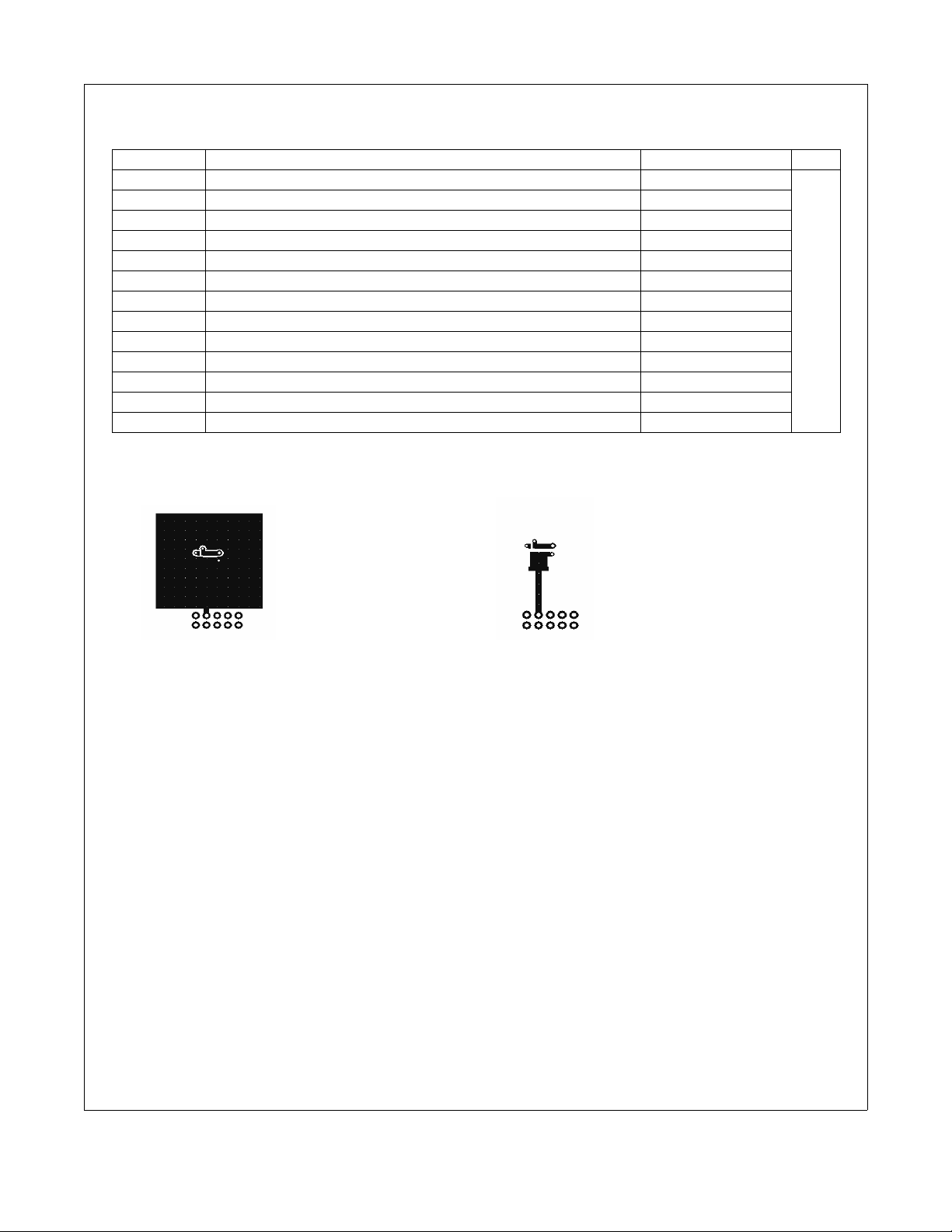
Package Marking and Ordering Information
©2010 Fairchild Semiconductor Corporation
FDMS2510SDC Rev.C
Device Marking Device Package Reel Size Tape Width Quantity
Thermal Resistance, Junction to Case (Top Source) 4.4
Thermal Resistance, Junction to Case (Bottom Drain) 2.1
Thermal Resistance, Junction to Ambient (Note 1a) 38
Thermal Resistance, Junction to Ambient (Note 1b) 81
Thermal Resistance, Junction to Ambient (Note 1i) 16
Thermal Resistance, Junction to Ambient (Note 1j) 23
Thermal Resistance, Junction to Ambient (Note 1k) 11
2510S FDMS2510SDC Dual Cool
TM
Power 56 13’’ 12 mm 3000 units
°C/W
www.fairchildsemi.com1
TM
FDMS2510SDC N-Channel Dual Cool
Electrical Characteristics T
= 25 °C unless otherwise noted
J
Symbol Parameter Test Conditions Min Typ Max Units
Off Characteristics
BV
ΔBV
ΔT
I
DSS
I
GSS
DSS
DSS
J
Drain to Source Breakdown Voltage ID = 1 mA, VGS = 0 V 25 V
Breakdown Voltage Temperature
Coefficient
Zero Gate Voltage Drain Current VDS = 20 V, V
Gate to Source Leakage Current, Forward VGS = 20 V, V
I
= 10 mA, referenced to 25 °C 19 mV/°C
D
= 0 V 500 μA
GS
= 0 V 100 nA
DS
On Characteristics
V
GS(th)
ΔV
ΔT
r
DS(on)
g
FS
GS(th)
J
Gate to Source Threshold Voltage VGS = VDS, ID = 1 mA 1.2 1.7 3.0 V
Gate to Source Threshold Voltage
Temperature Coefficient
Static Drain to Source On Resistance
I
= 10 mA, referenced to 25 °C -5 mV/°C
D
V
= 10 V, ID = 23 A 2.4 2.9
GS
= 4.5 V, ID = 18 A 3.4 4.2
GS
= 10 V, ID = 23 A, TJ = 125 °C 3.5 4.3
V
GS
Forward Transconductance VDS = 5 V, ID = 23 A 159 S
Dynamic Characteristics
C
iss
C
oss
C
rss
R
g
Input Capacitance
Output Capacitance 577 770 pF
Reverse Transfer Capacitance 128 195 pF
Gate Resistance 1.1 2.4 Ω
Switching Characteristics
t
d(on)
t
r
t
d(off)
t
f
Q
Q
Q
Q
g
g
gs
gd
Turn-On Delay Time
Rise Time 410ns
Turn-Off Delay Time 27 43 ns
Fall Time 310ns
Total Gate Charge VGS = 0 V to 10 V
Total Gate Charge VGS = 0 V to 4.5 V 15 21 nC
Gate to Source Gate Charge 6.3 nC
Gate to Drain “Miller” Charge 4.0 nC
= 13 V, VGS = 0 V,
V
DS
f = 1 MHz
= 13 V, ID = 23 A,
V
DD
V
= 10 V, R
GS
GEN
= 6 Ω
V
DD
I
= 23 A
D
= 13 V,
2090 2780 pF
10 20 ns
32 45 nC
mΩV
TM
PowerTrench
®
SyncFET
TM
Drain-Source Diode Characteristics
V
SD
t
rr
Q
rr
©2010 Fairchild Semiconductor Corporation
FDMS2510SDC Rev.C
Source to Drain Diode Forward Voltage
Reverse Recovery Time
Reverse Recovery Charge 17 31 nC
V
= 0 V, IS = 2 A (Note 2) 0.48 0.8
GS
= 0 V, IS = 23 A (Note 2) 0.79 1.2
V
GS
= 23 A, di/dt = 300 A/ μs
I
F
2
23 36 ns
V
www.fairchildsemi.com
Thermal Characteristics
FDMS2510SDC N-Channel Dual Cool
R
θJC
R
θJC
R
θJA
R
θJA
R
θJA
R
θJA
R
θJA
R
θJA
R
θJA
R
θJA
R
θJA
R
θJA
R
θJA
R
θJA
NOTES:
1. R
is determined with the device mounted on speci fi e d pa d 2 oz copper pad on board of FR-4 material. R
θJA
board design.
Thermal Resistance, Junction to Case (Top Source) 4.4
Thermal Resistance, Junction to Case (Bottom Drain) 2.1
Thermal Resistance, Junction to Ambient (Note 1a) 38
Thermal Resistance, Junction to Ambient (Note 1b) 81
Thermal Resistance, Junction to Ambient (Note 1c) 27
Thermal Resistance, Junction to Ambient (Note 1d) 34
Thermal Resistance, Junction to Ambient (Note 1e) 16
Thermal Resistance, Junction to Ambient (Note 1f) 19
Thermal Resistance, Junction to Ambient (Note 1g) 26
Thermal Resistance, Junction to Ambient (Note 1h) 61
Thermal Resistance, Junction to Ambient (Note 1i) 16
Thermal Resistance, Junction to Ambient (Note 1j) 23
Thermal Resistance, Junction to Ambient (Note 1k) 11
Thermal Resistance, Junction to Ambient (Note 1l) 13
a. 38 °C/W when mounted on
a 1 in2 pad of 2 oz copper
is guaranteed by design while R
θJC
b. 81 °C/W when mounted on
a minimum pad of 2 oz copper
is determined by the user's
θCA
°C/W
TM
PowerTrench
®
SyncFET
c. Still air, 20.9x10.4x12.7mm Aluminum Heat Sink, 1 in2 pad of 2 oz copper
d. Still air, 20.9x10.4x12.7mm Aluminum Heat Sink, minimum pad of 2 oz copper
e. Still air, 45.2x41.4x11.7mm Aavid Thermalloy Part # 10-L41B-11 Heat Sink, 1 in2 pad of 2 oz copper
f. Still air, 45.2x41.4x11.7mm Aavid Thermalloy Part # 10-L41B-11 Heat Sink, minimum pad of 2 oz copper
g. 200FPM Airflow, No Heat Sink,1 in2 pad of 2 oz copper
h. 200FPM Airflow, No Heat Sink, minimum pad of 2 oz copper
i. 200FPM Airflow, 20.9x10.4x12.7mm Aluminum Heat Sink, 1 in2 pad of 2 oz copper
j. 200FPM Airflow, 20.9x10.4x12.7mm Aluminum Heat Sink, minimum pad of 2 oz copper
k. 200FPM Airflow, 45.2x41.4x11.7mm Aavid Thermalloy Part # 10-L41B-11 Heat Sink, 1 in2 pad of 2 oz copper
l. 200FPM Airflow, 45.2x41.4x11.7mm Aavid Thermalloy Part # 10-L41B-11 Heat Sink, minimum pad of 2 oz copper
2. Pulse Test: Pulse Width < 300 μs, Duty cycle < 2.0%.
of 84 mJ is based on starting TJ = 25 °C, L = 1 mH, IAS = 13 A, VDD = 23 V, VGS = 10 V. 100% test at L = 0.3 mH, IAS = 20 A.
3. E
AS
4. As an N-ch device, the negative Vgs rating is for low duty cycle pulse ocurrence only. No continuous rating is implied.
5. ISD ≤ 23 A, di/dt ≤ 200 A/μs, VDD ≤ BV
, Starting TJ = 25 oC.
DSS
TM
©2010 Fairchild Semiconductor Corporation
FDMS2510SDC Rev.C
3
www.fairchildsemi.com