FDMS030N06B
N-Channel PowerTrench® MOSFET
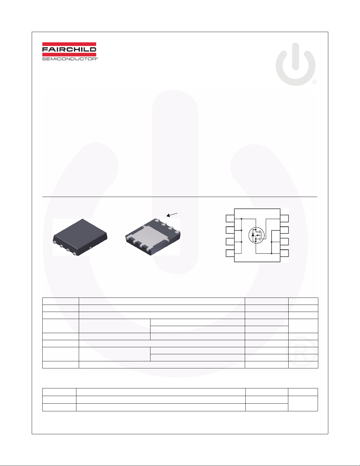
60 V, 100 A, 3 mΩ
FDMS030N06B — N-Channel PowerTrench
November 2013
Features
•R
• Advanced Package and Silicon Combination for Low R
• Fast Switching Speed
• 100% UIL Tested
• RoHS Compliant
= 2.4 mΩ (Typ.) @ VGS = 10 V, ID = 50 A
DS(on)
and High Efficiency
Top
Power 56
Bottom
D
D
D
D
DS(on)
S
Description
This N-Channel MOSFET is produced using Fairchild
Semiconductor’s advance PowerTrench
been tailored to minimize the on-state resistance while maintaining superior switching performance.
®
process that has
Applications
• Synchronous Rectification for ATX / Server / Telecom PSU
• Battery Protection Circuit
• Motor drives and Uninterruptible Power Supplies
• Renewable system
Pin 1
D
S
S
G
5
D
6
D
7
8
D
®
MOSFET
G
4
S
3
S
2
S
1
MOSFET Maximum Ratings T
Symbol Parameter FDMS030N06B Unit
V
V
I
I
E
P
T
D
DM
DSS
GSS
AS
D
, T
J
STG
Drain to Source Voltage 60 V
Gate to Source Voltage ±20 V
Drain Current
Drain Current - Pulsed (Note 3) 400 A
Single Pulsed Avalanche Energy (Note 4) 248 mJ
Power Dissipation
Operating and Storage Temperature Range -55 to +150
Thermal Characteristics
Symbol Parameter
R
θJC
R
θJA
©2010 Fairchild Semiconductor Corporation
FDMS030N06B Rev. C1
Thermal Resistance, Junction to Case, Max. 1.2
Thermal Resistance, Junction to Ambient, Max. (Note 2a) 50
= 25oC unless otherwise noted.
C
- Continuous (T
- Continuous (T
(T
= 25oC) 104 W
C
= 25oC) (Note 2a) 2.5 W
(T
A
= 25oC) (Note1) 100
C
= 25oC) (Note 2a) 22.1
A
1
FDMS030N06B
A
o
C
Unit
o
C/W
www.fairchildsemi.com

Package Marking and Ordering Information
Device Marking Device Package Reel Size Tape Width Quantity
FDMS030N06B FDMS030N06B Power 56 13 ” 12 mm 3000 units
FDMS030N06B — N-Channel PowerTrench
Electrical Characteristics
TC = 25oC unless otherwise noted.
Symbol Parameter Test Conditions Min. Typ. Max. Unit
Off Characteristics
BV
ΔBV
/ ΔT
I
DSS
I
GSS
DSS
DSS
J
Drain to Source Breakdown Voltage ID = 250 μA, VGS = 0V 60 - - V
Breakdown Voltage Temperature
Coefficient
Zero Gate Voltage Drain Current VDS = 48 V, V
Gate to Body Leakage Current VGS = ±20 V, V
I
= 250 μA, Referenced to 25oC - 0.03 - V/oC
D
= 0 V - - 1 μA
GS
= 0 V - - ±100 nA
DS
On Characteristics
V
GS(th)
R
DS(on)
g
FS
Gate Threshold Voltage VGS = VDS, ID = 250 μA 2.5 3.3 4.5 V
Static Drain to Source On Resistance VGS = 10 V, ID = 50 A - 2.4 3.0 mΩ
V
Forward Transconductance
= 10 V, ID = 50 A
DS
-119 - S
Dynamic Characteristics
C
iss
C
oss
C
rss
(er) Engry Releted Output Capacitance VDS = 30 V, VGS = 0 V - 2504 - pF
C
oss
Q
g(tot)
Q
gs
Q
gd
V
plateau
Q
sync
Q
oss
Input Capacitance
Output Capacitance - 1720 2290 pF
Reverse Transfer Capacitance - 59 - pF
= 30 V, VGS = 0 V
V
DS
f = 1 MHz
Total Gate Charge at 10V
V
= 30 V, ID = 50 A
Gate to Source Gate Charge - 30 - nC
Gate to Drain “Miller” Charge - 14 -nC
Gate Plateau Volatge - 5.4 -V
Total Gate Charge Sync.
DS
V
= 0 V to 10 V
GS
(Note 5)
V
= 0 V, ID = 50 A
DS
Output Charge VDS = 30 V, VGS = 0 V - 174 - nC
ESR Equivalent Series Resistance f = 1 MHz - 1.05 - Ω
- 5685 7560 pF
-75-nC
- 66.2 - nC
®
MOSFET
Switching Characteristics
t
d(on)
t
r
t
d(off)
t
f
Turn-On Delay Time
Turn-On Rise Time - 20 50 ns
Turn-Off Delay Time - 52 114 ns
Turn-Off Fall Time - 16 42 ns
= 30 V, ID = 50 A
V
DD
V
= 10 V, RG = 4.7 Ω
GS
(Note 5)
Drain-Source Diode Characteristics
I
S
I
SM
V
SD
t
rr
Q
rr
Notes:
1. Silicon limited I
2. R
is determined with the device mounted on a 1in2 pad 2 oz copper pad on a 1.5 x 1.5 in. board of FR-4 material. R
θJA
the user's board design.
3. Repetitive rating: pulse-width limited by maximum junction temperature.
4. L = 0.3 mH, I
5. Essentially independent of ope rating temperature typical character istics.
Maximum Continuous Drain to Source Diode Forward Current - - 100 A
Maximum Pulsed Drain to Source Diode Forward Current - - 400 A
Drain to Source Diode Forward Voltage VGS = 0 V, I
Reverse Recovery Time
Reverse Recovery Charge - 85 - nC
rating = 147 A.
D
a. 50 °C/W when mounted on a
2
1 in
pad of 2 oz copper.
= 40.7 A, VDD = 50 V, VGS = 10 V, starting TJ = 25°C.
AS
V
= 0 V, I
GS
dI
/dt = 100 A/μs
F
= 50 A - - 1.25 V
SD
= 50 A
SD
-3988ns
-71-ns
is guaranteed by design while R
θJC
b. 125 °C/W when mounted on a
minimum pad of 2 oz copper.
is determined by
θCA
©2010 Fairchild Semiconductor Corporation
FDMS030N06B Rev. C1
2
www.fairchildsemi.com

Typical Performance Characteristics
34567
1
10
100
500
-55oC
150oC
*Notes:
1. V
DS
= 10V
2. 250
μs Pulse Test
25oC
I
D
, Drain Current[A]
VGS, Gate-Source Voltage[V]
0.05 0.1 1 3
1
10
100
200
*Notes:
1. 250
μs Pulse Test
2. T
C
= 25oC
I
D
, Drain Current[A]
V
, Drain-Source Voltage[V]
V
GS
= 15.0V
10.0V
8.0V
7.0V
6.5V
6.0V
5.5V
5.0V
0 50 100 150 200
1.0
1.5
2.0
2.5
3.0
3.5
*Note: TC = 25oC
VGS = 20V
VGS = 10V
R
DS(ON)
[mΩ],
Drain-Source On-Resistance
ID, Drain Current [A]
0.2 0.4 0.6 0.8 1.0 1.2 1.4
1
10
100
500
*Notes:
1. VGS = 0V
2. 250
μs Pulse Test
150oC
I
S
, Reverse Drain Current [A]
VSD, Body Diode Forward Voltage [V]
25oC
0 153045607590
0
2
4
6
8
10
*Note: ID = 50A
VDS = 12V
V
DS
= 30V
V
DS
= 48V
V
GS
, Gate-Source Voltage [V]
Qg, Total Gate Charge [nC]
0.1 1 10 60
10
100
1000
10000
C
oss
C
iss
C
iss
= Cgs + Cgd (Cds = shorted)
C
oss
= Cds + C
gd
C
rss
= C
gd
*Note:
1. V
GS
= 0V
2. f = 1MHz
C
rss
Capacitances [pF]
VDS, Drain-Source Voltage [V]
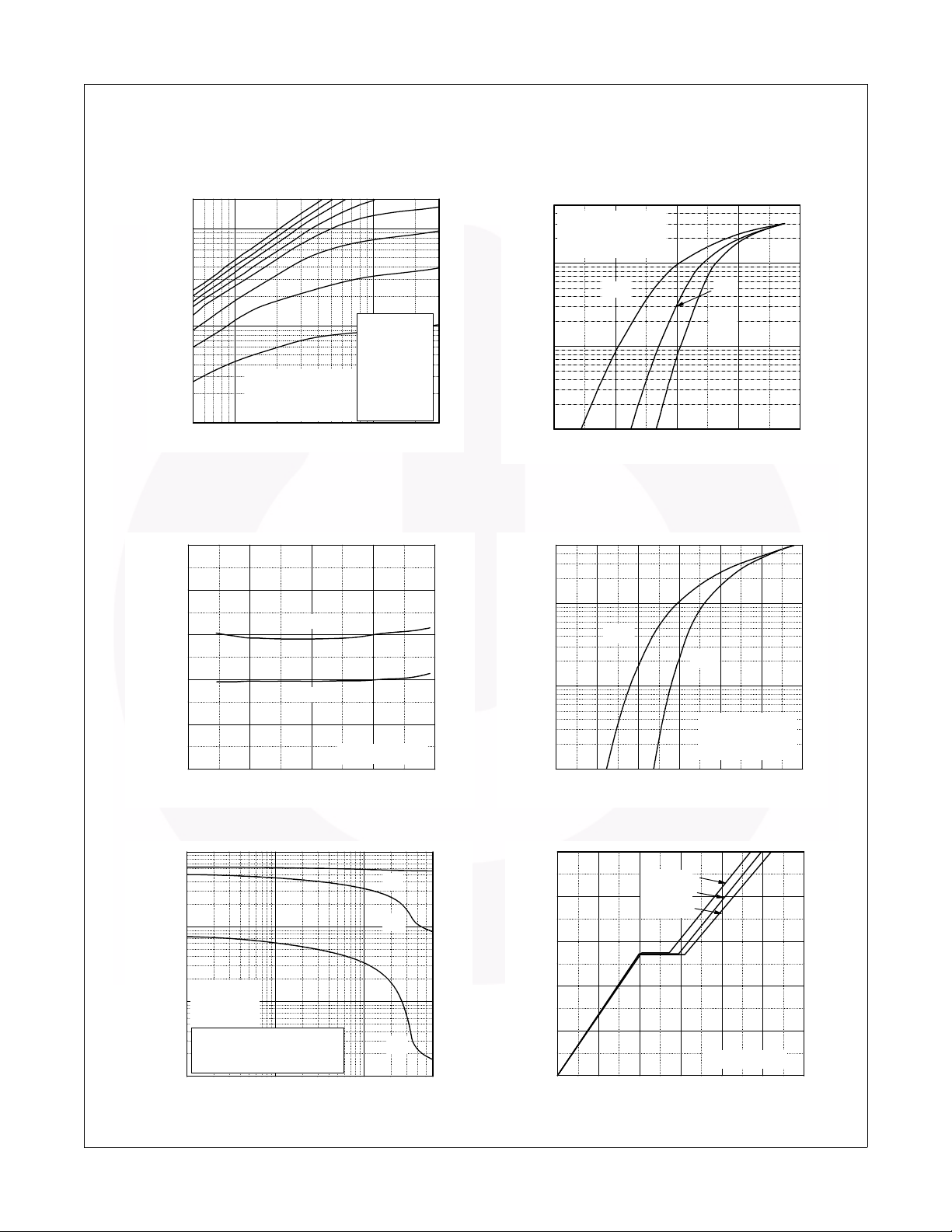
Figure 1. On-Region Characteristics Figure 2. Transfer Characteristics
Figure 3. On-Resistance Variation vs. Figure 4. Body Diode Forward Voltage
Drain Current and Gate Voltage Variation vs. Source Current
and Temperature
FDMS030N06B — N-Channel PowerTrench
®
MOSFET
Figure 5. Capacitance Characteristics Figure 6. Gate Charge Characteristics
©2010 Fairchild Semiconductor Corporation
FDMS030N06B Rev. C1
3
www.fairchildsemi.com

Typical Performance Characteristics (Continued)
-80 -40 0 40 80 120 160
0.94
0.96
0.98
1.00
1.02
1.04
1.06
*Notes:
1. V
GS
= 0V
2. I
D
= 250μA
BV
DSS
, [Normalized]
Drain-Source Breakdown Voltage
TJ, Junction Temperature [oC]
-80 -40 0 40 80 120 160
0.6
0.8
1.0
1.2
1.4
1.6
1.8
*Notes:
1. V
GS
= 10V
2. I
D
= 50A
R
DS(on)
, [Normalized]
Drain-Source On-Resistance
TJ, Junction Temperature [oC]
25 50 75 100 125 150
0
30
60
90
120
150
I
D
, Drain Current [A]
TC, Case Temperature [oC]
VGS= 10V
R
θJC
= 1.2oC/W
0.01 0.1 1 10 100
0.01
0.1
1
10
100
1000
1ms
10ms
100ms
I
D
, Drain Current [A]
VDS, Drain-Source Voltage [V]
Operation in This Area
is Limited by R
DS(on)
*Notes:
1. T
a
= 25oC
2. T
J
= 150oC
3. Single Pulse
DC
0 102030405060
0
0.5
1.0
1.5
2.0
2.5
3.0
E
OSS
, [μJ]
VDS, Drain to Source Voltage [V]
0.001 0.01 0.1 1 10 100 1,000
1
10
100
TJ = 25
o
C
TJ = 125oC
I
AS
, Avalanche Current [A]
tAV, Time In Avalanche [ms]
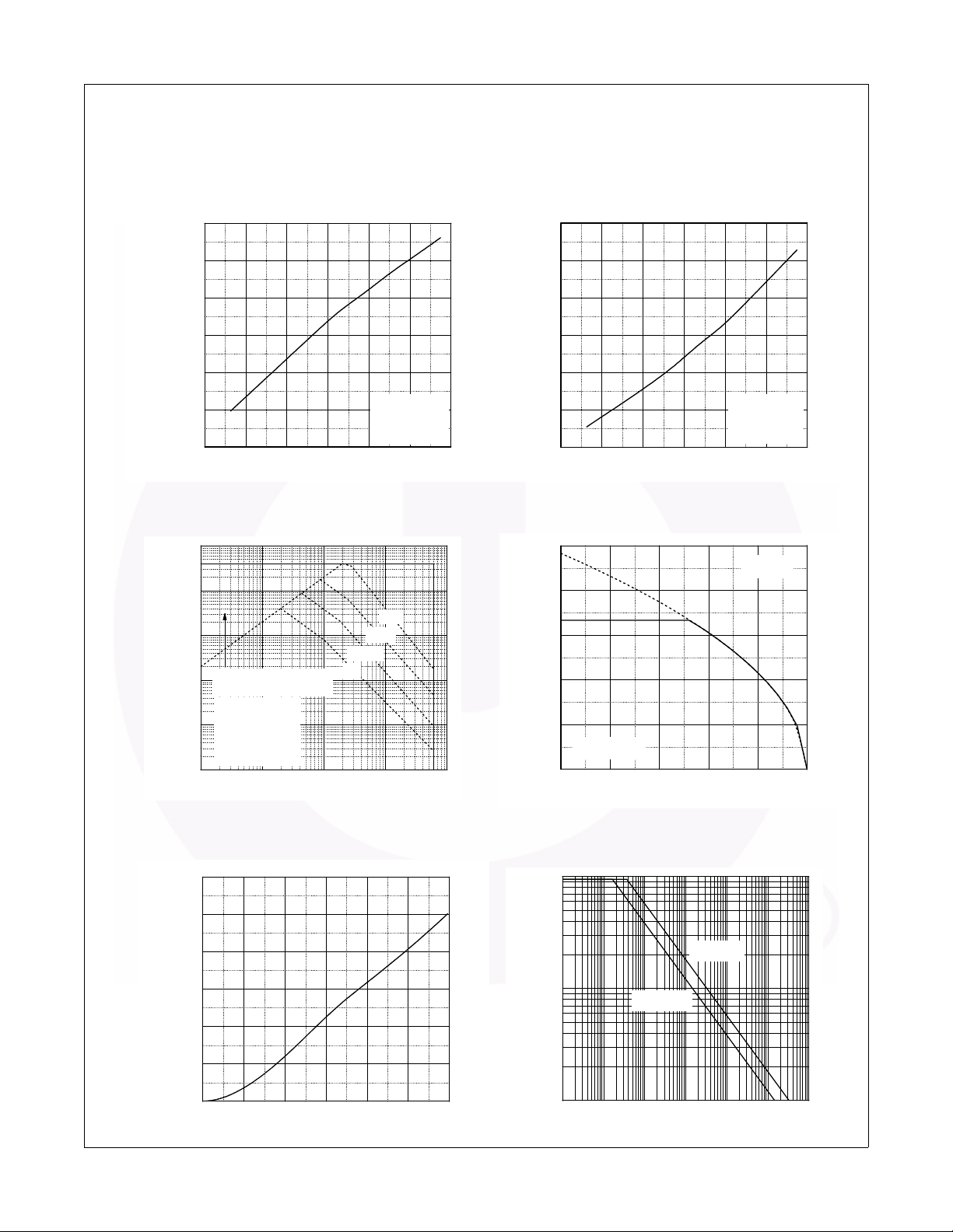
Figure 7. Breakdown Voltage Variation Figure 8. On-Resistance Variation
vs. Temperature vs. Temperature
Figure 9. Maximum Safe Operating Area Figure 10. Maximum Drain Current
vs. Case Temperature
FDMS030N06B — N-Channel PowerTrench
®
MOSFET
Figure 11. Eoss vs. Drain to Source Voltage Figure 12. Unclamped Inductive
Switching Capability
©2010 Fairchild Semiconductor Corporation
FDMS030N06B Rev. C1
4
www.fairchildsemi.com
 Loading...