Fairchild FDMQ8403 service manual

FDMQ8403
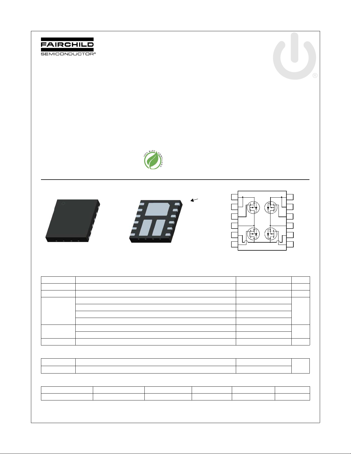
Bottom
MLP 4.5x5
Top
4
3
2
1
9
10
11
12
5
6
8
7S3
S3
G3
D3/S4
D1/D4
G4
S2
S2
G2
D1/D4
G1
S1/D2
Q4Q3Q1
Q2
S2
S1/D2
G2
S2
D1/D4
G1
S3
D3/S4
G3
S3
D1/D4
G4
Pin 1
S1/
D2
D1/D4
D3/
S4
GreenBridgeTM Series of High-Efficiency Bridge Rectifiers
®
N-Channel PowerTrench
100 V, 6 A, 110 mΩ
Features
Max r
Max r
Substantial efficiency benefit in PD solutions
RoHS Compliant
= 110 mΩ at VGS = 10 V, ID = 3 A
DS(on)
= 175 mΩ at VGS = 6 V, ID = 2.4 A
DS(on)
MOSFET
General Description
This quad MOSFET solution provides ten-fold improvement in
power dissipation over diode bridge.
Application
High-Efficiency Bridge Rectifiers
FDMQ8403 Dual N-Channel PowerTrench
December 2011
®
MOSFET
MOSFET Maximum Ratings T
= 25 °C unless otherwise noted
A
Symbol Parameter Ratings Units
V
DS
V
GS
Drain to Source Voltage 100 V
Gate to Source Voltage ±20 V
Drain Current -Continuous (Package limited) TC = 25 °C 6
I
D
-Continuous (Silicon limited) T
-Continuous T
= 25 °C 9
C
= 25 °C (Note 1a) 3.1
A
A
-Pulsed 12
P
D
, T
T
J
STG
Power Dissipation TC = 25 °C 17
Power Dissipation T
= 25 °C (Note 1a) 1.9
A
W
Operating and Storage Junction Temperature Range -55 to +150 °C
Thermal Characteristics
R
θJA
R
θJA
Package Marking and Ordering Information
Device Marking Device Package Reel Size Tape Width Quantity
©2011 Fairchild Semiconductor Corporation
FDMQ8403 Rev.C1
FDMQ8403 FDMQ8403 MLP 4.5x5 13 ’’ 12 mm 3000 units
Thermal Resistance, Junction to Ambient (Note 1a) 65
Thermal Resistance, Junction to Ambient (Note 1b) 135
1
°C/W
www.fairchildsemi.com

FDMQ8403 Dual N-Channel PowerTrench
Electrical Characteristics T
= 25 °C unless otherwise noted
J
Symbol Parameter Test Conditions Min Typ Max Units
Off Characteristics
BV
ΔBV
ΔT
I
DSS
I
GSS
DSS
DSS
J
Drain to Source Breakdown Voltage ID = 250 μA, VGS = 0 V 100 V
Breakdown Voltage Temperature
Coefficient
Zero Gate Voltage Drain Current VDS = 80 V, V
Gate to Source Leakage Current VGS = ±20 V, V
I
= 250 μA, referenced to 25 °C 72 mV/°C
D
= 0 V 1 μA
GS
= 0 V ±100 nA
DS
On Characteristics
V
GS(th)
ΔV
ΔT
r
DS(on)
g
FS
GS(th)
J
Gate to Source Threshold Voltage VGS = VDS, ID = 250 μA22.84V
Gate to Source Threshold Voltage
Temperature Coefficient
Static Drain to Source On Resistance
I
= 250 μA, referenced to 25 °C -8 mV/°C
D
V
= 10 V, ID = 3 A 85 110
GS
= 6 V, ID = 2.4 A 115 175
GS
= 10 V, ID = 3 A, TJ = 125 °C 147 191
V
GS
Forward Transconductance VDS = 10 V, ID = 3 A 6 S
Dynamic Characteristics
C
iss
C
oss
C
rss
Input Capacitance
Output Capacitance 43 60 pF
Reverse Transfer Capacitance 2.6 5 pF
Switching Characteristics
t
d(on)
t
r
t
d(off)
t
f
Q
Q
Q
Q
g
g
gs
gd
Turn-On Delay Time
Rise Time 1.2 10 ns
Turn-Off Delay Time 7.2 15 ns
Fall Time 1.8 10 ns
Total Gate Charge VGS = 0 V to 10 V
Total Gate Charge VGS = 0 V to 5 V 1.7 3 nC
Gate to Source Charge 0.9 nC
Gate to Drain “Miller” Charge 0.8 nC
= 50 V, VGS = 0 V,
V
DS
f = 1 MHz
= 50 V, ID = 3 A,
V
DD
V
= 10 V, R
GS
GEN
= 6 Ω
V
DD
I
= 3 A
D
= 50 V,
162 215 pF
4.1 10 ns
35nC
mΩV
®
MOSFET
Drain-Source Diode Characteristics
V
SD
t
rr
Q
rr
Notes:
1. R
is determined with the device mounted on a 1 in2 pad 2 oz copper pad on a 1.5 x 1.5 in. board of FR- 4 mater ial. R
θJA
the user's board design.
2. Pulse Test: Pulse Width < 300 μs, Duty cycle < 2.0%.
©2011 Fairchild Semiconductor Corporation
FDMQ8403 Rev.C1
Source to Drain Diode Forward Voltage V
Reverse Recovery Time
Reverse Recovery Charge 23 37 nC
a. 65 °C/W when mounted on a 1 in
I
F
pad of 2 oz copper. the board
designed Q1+Q3 or Q2+Q4.
= 0 V, IS = 3 A (Note 2) 0.86 1.3 V
GS
= 3 A, di/dt = 100 A/μs
2
2
is guaranteed by design while R
θJC
b. 135 °C/W when mounted on a
minimum pad of 2 oz copper.
the board designed Q1+Q3 or
Q2+Q4.
33 53 ns
is determined by
θCA
www.fairchildsemi.com
 Loading...