Fairchild FDMF6730 service manual

FDMF6730
PWM
CONTROLLER
LDO O UT
LDO E NABLE
LDO 5V OUT
PW M OUT
VIN
VOUT
DR IVE LS
DR IVE HS
LDO ADJ
LDO OUT
LDO EN
LDO 5V
VC C VIN
BOO T
VS WH
PG ND
LDR V
G_ PASS
D_P ASS
S_P ASSCS_ PROG
CS_ OUT
CG ND
FDMF6730
PWM
CONTROLLER
LDO O UT
LDO E NABLE
LDO 5V OUT
PW M OUT
VIN
VOUT
DR IVE LS
DR IVE HS
LDO ADJ
LDO OUT
LDO EN
LDO 5V
VC C VIN
BOO T
VS WH
PG ND
LDR V
G_ PASS
D_P ASS
S_P ASSCS_ PROG
CS_ OUT
CG ND
FDMF6730
Driver plus FET Multi-chip Module
FDMF6730 Driver plus FET Multi-chip Module
August 2008
Features
Over 95% efficiency
Internal 5V regulator for gate drive
6V-16V input range
1MHz max operating frequency
SMOD operation capability for light load efficiency
5A current capability (10A with PASS FET)
Current limit set by R
sensing to minimize power losses
DSON
Integrated bootstrap diode
Applications
Ultra Mobile PC
Notebook Computers
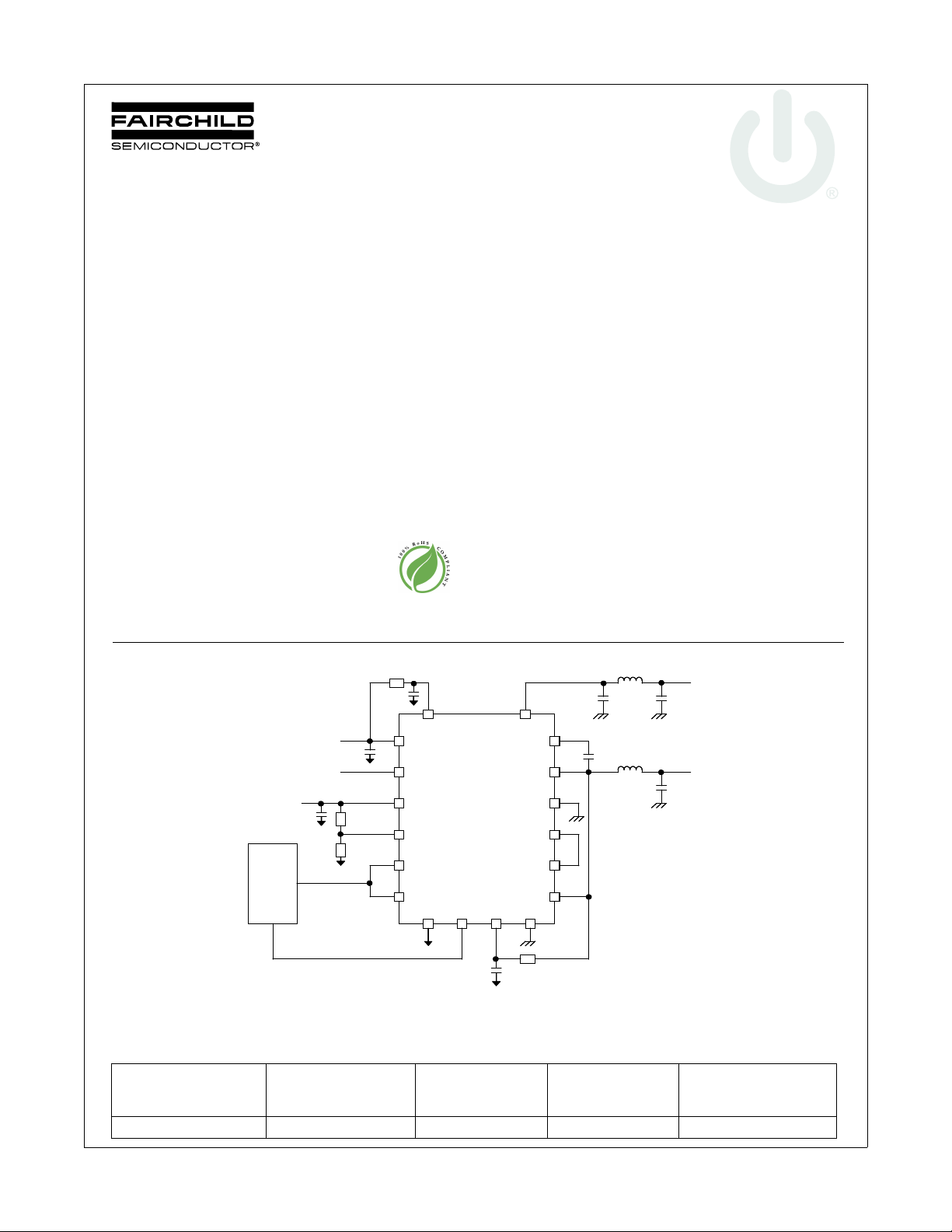
Typical Application
General Description
The FDMF6730 is a high efficiency Driver plus MOSFET power
stage solution optimized for Ultra Mobile PC (UMPC) system
power voltage supplies. It is fully compliant with the Intel UltraMobile Driver MOS (uDrMOS) Specification. The MOSFETs and
driver have been optimized to perform with high efficiency at
light and medium loads, ideal for compact PC devices.
The internal driver IC integrates two highly efficient LDOs for
internal gate-drive and external circuitry. The bootstrap diode is
also integrated within the IC. When operating with a single low
side MOSFET the uDrMOS module is capable of delivering up
to 5A of continuous current. The PASS transistor may be easily
routed in parallel with the low side MOSFET to provide up to
10A. The module also incorporates an over current protection
flag from an R
The device comes in a 6X6 Power QFN package for improved
thermal performance.
current sense architecture.
DSON
Ordering Information
©2008 Fairchild Semiconductor Corporation
Part
FDMF6730 10 6-16 1000 FDMF6730
FDMF6730 Rev. D2
Current Rating
Max
[A]
Figure 1. Power Train Application Circuit
Input Voltage
Typical
[V]
Frequency
Max
[KHz]
1
Device
Marking
www.fairchildsemi.com

Functional Block Diagram
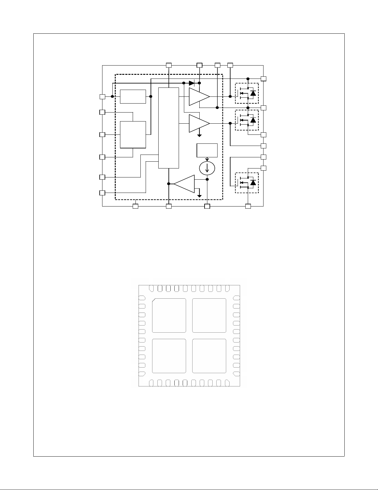
Figure 2. Functional Block Diagram
5V Reg
LD O
Ad just
OC P
Current
Tr im min g
VCC BOOT PHASE
VIN
VSW H
PGND
LD RV
G_PASS
D_PA S S
HD RV
S_PASSCS_P R O GCS _OUTCGND
DRIV E _ LS
DRIV E _ H S
LD O _ADJ
LD O_OUT
LD O _EN
LD O _5V
5V Reg
LD O
Ad just
OC P
Current
Tr im min g
VCC BOOT PHASE
VIN
VSW H
PGND
LD RV
G_PASS
D_PA S S
HD RV
S_PASSCS_P R O GCS _OUTCGND
DRIV E _ LS
DRIV E _ H S
LD O _ADJ
LD O_OUT
LD O _EN
LD O _5V
Figure 3. 6mm X 6mm, 40L MLP Bottom View
PGND
VSWH
VSWH
VSWH
VSWH
VIN
VIN
VIN
VIN
VIN
10
PGND
PGND
PGND
LDRV
VSWH
D_PASS
G_PASS
S_PASS
S_PASS
S_PASS
31
40
1
A
(VSWH)
S_PASS
NC
D_PASS
CS_PROG
CS_OUT
VCC
CGND
DRIVE_HS
DRIVE_LS
LDO_EN
2130
VIN
VIN
HDRV
CGND
PHASE
BOOT
LDO_5V
LDO_OUT
LDO_ADJ
20
11
VIN
B
(VIN)
D
(D_PASS)
C
(CGND)
PGND
VSWH
VSWH
VSWH
VSWH
VIN
VIN
VIN
VIN
VIN
10
PGND
PGND
PGND
LDRV
VSWH
D_PASS
G_PASS
S_PASS
S_PASS
S_PASS
31
40
1
A
(VSWH)
S_PASS
NC
D_PASS
CS_PROG
CS_OUT
VCC
CGND
DRIVE_HS
DRIVE_LS
LDO_EN
2130
VIN
VIN
HDRV
CGND
PHASE
BOOT
LDO_5V
LDO_OUT
LDO_ADJ
20
11
VIN
B
(VIN)
D
(D_PASS)
C
(CGND)
FDMF6730 Driver plus FET Multi- chip Module
Pin Configuration
FDMF6730 Rev. D2
2
www.fairchildsemi.com

Pin Description
Pin Name Function
1, 38 - 40 PGND Low Side FET Source Pin. Connect to GND
2 - 5, 36, A VSWH Switch Node Pin. Low Side FET Drain pin. Electrically shorted to PHASE pin
6 - 12,14,B VIN Input Voltage Pin. Input voltage for buck converter
13 HDRV HDRV pin. High Side driver output. Connected to High Side FET gate pin.
15, 24, C CGND IC Ground. Ground return for driver IC.
16 PHASE Switch Node Pin for easy bootstrap capacitor routing. Electrically shorted to VSWH pin.
17 BOOT Bootstrap Supply Input Pin. Provides voltage supply to high-side MOSFET driver. Connect
bootstrap capacitor.
18 LDO_5V 5V Internal LDO Output.
19 LDO_OUT Adjustable LDO Output.
20 LDO_ADJ LDO Adjust Input. Connect to external voltage divider to adjust LDO output.
21 LDO_EN Adjustable LDO Enable Pin. 1 = Enable, 0 = Disable
22 DRIVE_LS Low Side PWM Input. Connect to PWM controller.
23 DRIVE_HS High Side PWM Input. Connect to PWM controller.
25 VCC Driver VCC. Connect to 5V.
26 CS_OUT Current Sense Output. 1 = Over-current Fault, 0 = No Fault.
27 CS_PROG Current Sense Program.
28, 35, D D_PASS Pass FET Drain Pin. Connect to VSWH pad for higher output current.
29 NC No Connect. This pin must be floated. Must not be connected to any pin.
30-33 S_PASS Pass FET Source Pin. Connect to PGND pad for higher output current.
34 G_PASS Pass FET Gate Pin. Connect to LDRV pin for higher output current.
37 LDRV LDRV pin. Low Side driver output. Connect to G_PASS pin for higher output current.
FDMF6730 Driver plus FET Multi- chip Module
Absolute Maximum Rating
Stresses exceeding the absolute maximum rating may damage the device. The device may not function or be operable above the
recommended operating conditions and stressing these parts to these levels is not recommended. In addition, extended exposure to
stresses above the recommended operating conditions may affect the device reliability. The absolute maximum rating are stress ratings only.
Parameter Min. Max. Units
VCC, Drive_LS, Drive_HS, LDO_EN, CS_Prog, CS_Out to GND -0.3 6 V
VIN to PGND -0.3 20 V
BOOT to VSWH -0.3 6 V
VSWH to PGND -1.0 27 V
BOOT to PGND -0.3 27 V
I
O(AV)
I
O(PK)
R
θJPCB
P
T
Operating and Storage Junction Temperature Range -55 150 °C
Note 1: Package power dissipation based on 4 layer, 2 square inch, 2 oz. copper pad. R
thermal resistance with PCB temperature referenced at VSWH pin.
VIN = 8.4V, VO = 3.3V, fSW = 1MHz, T
VIN = 8.4V, t
Junction to PCB Thermal Resistance note 1.
T
=130°C
PCB
= 10s 35 A
PULSE
= 130°C 10 A
PCB
5.5 °C/W
3.3 W
is the steady state junction to PCB
θJPCB
FDMF6730 Rev. D2
3
www.fairchildsemi.com
 Loading...