Fairchild FDMF6704V service manual

tm
August 2009
FDMF6704V - XSTM DrMOS
The Xtra Small, High Performance, High Frequency DrMOS Module with LDO
FDMF6704V - XS
Benefits
Single 12 V power supply operation.
Ultra compact size - 6 mm x 6 mm MLP, 44 % space
saving compared to conventional MLP 8 mm x 8 mm
DrMOS packages.
Ultra compact thermally enhanced 6 mm x 6 mm MLP
package 84 % smaller than conventional discrete solutions.
Fully optimized system efficiency.
Clean voltage waveforms with reduced ringing.
High frequency operation.
Compatible with a wide variety of PWM controllers in the
market.
Single input voltage operation.
Features
Internal 12 V to 5 V regulator.
Synchronous driver plus FET multichip module.
High current handling of 35 A.
Over 93 % peak efficiency.
Tri-State PWM input.
Fairchild's PowerTrench® 5 technology MOSFETs for clean
voltage waveforms and reduced ringing.
Optimized for high switching frequencies of up to 1 MHz.
Skip mode SMOD [low side gate turn off] input.
Fairchild SyncFETTM [integrated Schottky diode] technology
in the low side MOSFET.
Integrated bootstrap Schottky diode.
Adaptive gate drive timing for shoot-through protection.
Driver output disable function [DISB# pin].
Undervoltage lockout (UVLO).
Fairchild Green Packaging and RoHS
compliant. Low profile SMD package.
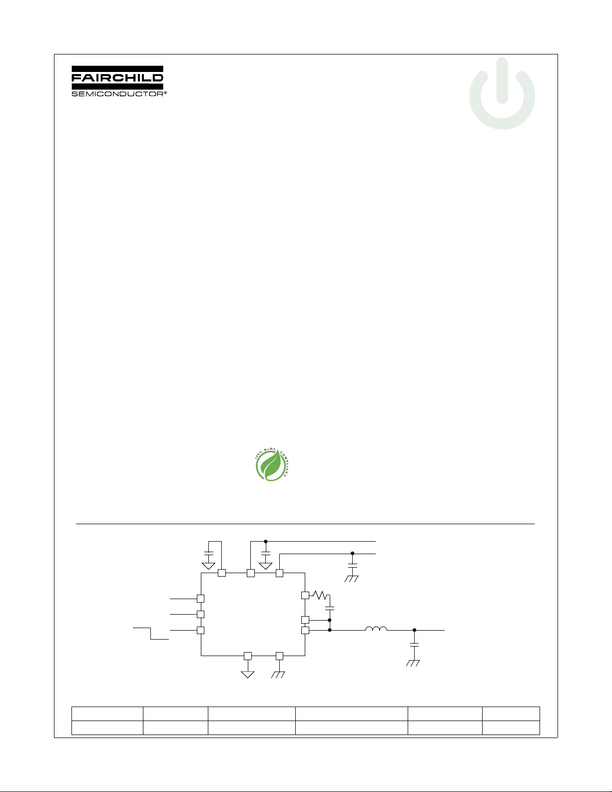
Power Train Application Circuit
C
VDRV
VIN
BOOT
PHASE
VSWH
DISB#
PWM Input
OFF
ON
C
VCIN
VCIN
DISB#
PWM
SMOD#
VDRV
CGND PGND
General Description
The XSTM DrMOS family is Fairchild’s next-generation fullyoptimized, ultra-compact, integrated MOSFET plus driver power
stage solutions for high current, high frequency synchronous
buck DC-DC applications. The FDMF6704V XSTM DrMOS
integrates a driver IC, two power MOSFETs and a bootstrap
Schottky diode along with an integrated 5 V gate drive LDO
regulator into a thermally enhanced, ultra compact 6 mm x 6
mm MLP package. With an integrated approach, the complete
switching power stage is optimized with regards to driver and
MOSFET dynamic performance, system inductance and
R
. This greatly reduces the package parasitics and layout
DS(ON)
challenges associated with conventional discrete solutions.
XSTM DrMOS uses Fairchild's high performance
PowerTrenchTM 5 MOSFET technology, which dramatically
reduces ringing in synchronous buck converter applications.
PowerTrench
buck converter applications. The driver IC incorporates
advanced features such as SMOD for improved light load
efficiency and a Tri-State PWM input for compatibility with a
wide range of PWM controllers. A 5 V gate drive and an
improved PCB interface, optimized for a maximum low side FET
exposed pad area, ensure higher performance. This product is
compatible with the new Intel 6 mm x 6 mm DrMOS
specification.
TM
5 can eliminate the need for a snubber circuit in
Applications
Compact blade servers V-core, non V-core and VTT DC-DC
converters.
Desktop computers V-core, non V-core and VTT DC-DC
converters.
Workstations V-core, non V-core and VTT DC-DC
converters.
Gaming Motherboards V-core, non V-core and VTT DC-DC
converters.
Gaming consoles.
High-current DC-DC Point of Load (POL) converters.
Networking and telecom microprocessor voltage regulators.
V
DRV
V
IN
C
VIN
R
BOOT
C
BOOT
L
OUT
OUTPUT
C
OUT
TM
DrMOS with Internal 5V Regulator
Figure 1. Power Train Application Circuit
Ordering Information
Order Number Marking Temperature Range Device Package Packing Method Quantity
FDMF6704V FDMF6704V_1 -55 °C to 150 °C 40 Pin, 3 DAP, MLP 6x6 mm Tape and Reel 3000
©2008 Fairchild Semiconductor Corporation
FDMF6704V Rev.C
1
www.fairchildsemi.com

Functional Block Diagram
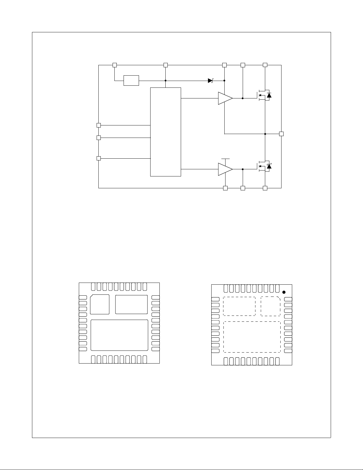
Figure 2. Functional Block Diagram
CGND
PGND
VSWH
VIN
BOOT
VCIN
VCIN
GH
GL
VDRV
PWM
DISB#
Overlap
Control
SMOD#
Q1
Q2
5 V
Reg
CGND
VIN
VSWH
Figure 3. 6mm x 6mm, 40L MLP
CGND
VIN
VSWH
PWM
SMOD#
DISB#
NC
CGND
GL
VSWH
VSWH
VSWH
VSWH
VSWH
VCIN
VDRV
BOOT
CGND
GH
NC
VIN
VIN
VIN
VIN
VIN
VIN
VSWH
PGND
VSWH
VSWH
PGND
PGND
PGND
PGND
PGND
PGND
PGND
PHASE
PGND
PGND
PGND
PGND
PGND
Bottom View Top View
1
2
3
4
5
6
7
8
9
10
11
12
13
14
15
16
17
18
19
20
30
29
28
27
26
25
24
23
22
21
40
39
38
37
36
35
34
33
32
31
123456789
10
40
39
38
37
36
35
34
33
32
31
302928272625242322
21
11
12
13
14
15
16
17
18
19
20
SMOD#
VCIN
VDRV
BOOT
CGND
GH
NC
VIN
VIN
PHASE
VIN
VIN
VIN
VIN
VSWH
PGND
PGND
PGND
PGND
PGND
PGND
VSWH
VSWH
PGND
PGND
PGND
PGND
PGND
PGND
PGND
PWM
DISB#
NC
CGND
GL
VSWH
VSWH
VSWH
VSWH
VSWH
41
42
43
41
42
43
FDMF6704V - XS
TM
DrMOS with Internal 5V Regulator
Pin Configuration
FDMF6704V Rev. C
2
www.fairchildsemi.com

Pin Description
Pin Name Function
When SMOD# = HI, low side driver is inverse of PWM input. When SMOD# = Low, low
1 SMOD#
2 VCIN
3 VDRV
4 BOOT
5, 37, 41 CGND IC Ground. Ground return for driver IC.
6 GH For manufacturing test only. This pin must be floated. Must not be connected to any pin.
7 PHASE Switch node pin for easy bootstrap capacitor routing. Electrically shorted to VSWH pin.
8, 38 NC Not Connected Internally.
9-14, 42 VIN Power input. Output stage supply voltage.
15, 29-35, 43 VSWH
16-28 PGND Power Ground. Output stage ground. Source pin of low side MOSFET(s).
36 GL For manufacturing test only. This pin must be floated. Must not be connected to any pin.
39 DISB#
40 PWM
side driver is disabled. This pin has no internal pullup or pulldown. It should not be left
floating. Do not add noise filter cap.
Regulator 5 V Output. Power for gate drives and logic. A minimum 4.7 F X7R ceramic
capacitor is required to be connected from this pin to CGND.
Regulator Input Voltage. A minimum 4.7 F X7R ceramic capacitor is required to be
connected from this pin to CGND.
Bootstrap Supply Input. Provides voltage supply to high-side MOSFET driver. Connect
bootstrap capacitor from this pin to PHASE.
Switch Node Output. Provides return for high-side bootstrapped driver and acts as a
sense point for the adaptive shoot-thru protection.
Output disable. When low, this pin disable FET switching (GH and GL are held low). This
pin has no internal pullup or pulldown. It should not be left floating. Do not add noise filter
cap.
PWM Signal Input. This pin accepts a Tri-state logic-level PWM signal from the controller.
Do not add noise filter cap.
FDMF6704V - XS
TM
DrMOS with Internal 5V Regulator
Absolute Maximum Rating
Parameter Min Max Units
VCIN, DISB#, PWM, SMOD#, GL to CGND 6 V
VIN to PGND, CGND 27 V
VDRV to PGND, CGND 16 V
BOOT, GH to VSWH, PHASE 6 V
BOOT, VSWH, PHASE, GH to GND 27 V
BOOT to VCIN 22 V
I
* VIN = 12 V, VO = 1.3 V
O(AV)
I
* 80 A
O(peak)
R
θJB
Operating and Storage Junction Temperature Range -55 150 °C
* I
and I
O(AV)
O(peak)
Thermal Resistance Junction to Board 3.75 °C/W
are measured in FCS evaluation board. These ratings can be changed with different application setting.
fSW = 350 kHz 35 A
fSW = 1 MHz 32 A
Recommended Operating Range
Parameter Min Typ Max Units
V
DRV
V
IN
* May be operated at lower input voltage. See figure 10.
Vgate and Logic Supply Voltage 8 12 14 V
Output FET Supply Voltage 3* 12 14 V
FDMF6704V Rev. C
3
www.fairchildsemi.com

Electrical Characteristics
VIN = 12 V, V
Parameter Symbol Conditions Min Typ Max Units
Operating Quiescent Current IQ
Internal 5V Regulator
Input Voltage V
Input Current I
Output voltage V
Power Dissipation P
VCIN Capacitor C
Line Regulation 8V < V
Load Regulation V
Short Circuit Current Limit 200 mA
UVLO Threshold 7.5 V
UVLO COMP Hysteresis 0.5 V
PWM Input
Sink Impedance PWM to GND 10 k
Source Impedance PWM to V
Tri-State Rising Threshold 3.2 3.4 3.6 V
Tri-State Rising Hysteresis 100 mV
Tri-State Falling Threshold 1.2 1.4 1.6 V
Tri-State Falling Hysteresis 100 mV
Tri-State Pin Open 2.5 V
Tri-State Shut Off Time 100 ns
SMOD# and DISB# Input
High Level Input Voltage 2 V
Low Level Input Voltage 0.8 V
Input Bias Current -2 2 A
Propagation Delay Time
High Side Driver
Rise Time 10 % to 90 % 25 ns
Fall Time 90 % to 10 % 20 ns
Deadband Time t
Propagation Delay t
Low Side Driver
Rise Time 10 % to 90 % 25 ns
Fall Time 90 % to 10 % 20 ns
Deadband Time t
Propagation Delay t
250 ns Time Out Circuit
250 ns Time Delay
= 12 V, TA = 25 °C unless otherwise noted.
DRV
DRV
VDRV
CIN
VDRV
VCIN
DTHH
PDHL
DTLH
PDLL
PWM = GND 2
PWM = V
CIN
2
mA
8 14 V
8V < VIN < 14V, 1MHz 36 mA
V
= 8V, I
DRV
V
= 12V, 1MHz 250 mW
DRV
= 5mA 4.8 5 5.2 V
Load
X7R Ceramic 4.7 10 F
DRV
= 8V, 5mA < I
DRV
< 14V, I
CIN
= 5mA 20 mV
Load
< 100mA 75 mV
Load
10 k
PWM = GND, delay between SMOD#
or DISB# from HI to LO to GL from HI
15 ns
to LO.
GL going LO to GH going HI, 10 % to
10 %
25 ns
PMW going LO to GH going LO 10 ns
VSWH going LO to GL going HI, 10
% to 10 %
20 ns
PWM going HI to GL going LO 10 ns
Delay between GH from HI to LO and
GL from LO to HI if VSWH is high.
250 ns
FDMF6704V - XS
TM
DrMOS with Internal 5V Regulator
FDMF6704V Rev. C
4
www.fairchildsemi.com
 Loading...