FDME910PZT
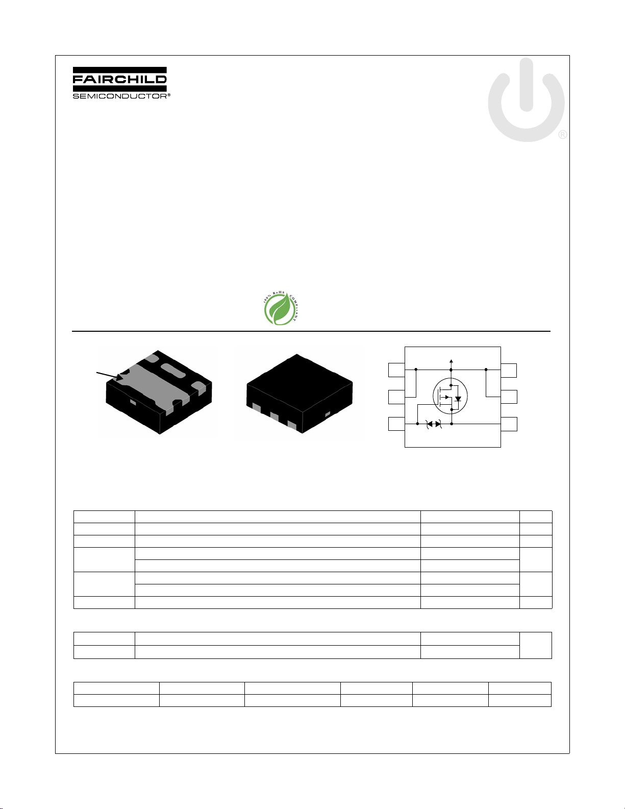
MicroFET 1.6x1.6 Thin
TOP
BOTTOM
Pin 1
D
G
D
S
D
D
5
1
6
2
3
4
D
D
S
D
D
G
Bottom Drain Contact
P-Channel PowerTrench® MOSFET
-20 V, -8 A, 24 mΩ
Features
Max r
Max r
Max r
Low profile: 0.55 mm maximum in the new package MicroFET
1.6x1.6 Thin
HBM ESD protection level > 2 kV typical (Note 3)
Free from halogenated compounds and antimony oxides
RoHS Compliant
= 24 mΩ at VGS = -4.5 V, ID = -8 A
DS(on)
= 31 mΩ at VGS = -2.5 V, ID = -7 A
DS(on)
= 45 mΩ at VGS = -1.8 V, ID = -6 A
DS(on)
General Description
This device is designed specifically for battery charging or load
switching in cellular handset and other ultraportable applications.
It features a MOSFET with low on-state resistance and zener
diode protection against ESD. The MicroFET 1.6x1.6 Thin
package offers exceptional thermal performance for its physical
size and is well suited to switching and linear mode applications.
FDME910PZT P-Channel PowerTrench
May 2012
®
MOSFET
MOSFET Maximum Ratings T
Symbol Parameter Ratings Units
V
DS
V
GS
I
D
P
D
, T
T
J
STG
Thermal Characteristics
R
θJA
R
θJA
Package Marking and Ordering Information
©2012 Fairchild Semiconductor Corporation
FDME910PZT Rev.C
Device Marking Device Package Reel Size Tape Width Quantity
Drain to Source Voltage -20 V
Gate to Source Voltage ±8 V
-Continuous TA = 25°C (Note 1a) -8
-Pulsed -32
Power Dissipation TA = 25°C (Note 1a) 2.1
Power Dissipation T
Operating and Storage Junction Temperature Range -55 to +150 °C
Thermal Resistance, Junction to Ambient (Note 1a) 60
Thermal Resistance, Junction to Ambient (Note 1a) 175
E91 FDME910PZT MicroFET 1.6x1.6 Thin 7 ’’ 8
= 25 °C unless otherwise noted
A
A
= 25°C (Note 1b) 0.7
A
W
°C/W
mm 5000 units
1
www.fairchildsemi.com

FDME910PZT P-Channel PowerTrench
Electrical Characteristics T
= 25 °C unless otherwise noted
J
Symbol Parameter Test Conditions Min Typ Max Units
Off Characteristics
BV
ΔBV
ΔT
I
DSS
I
GSS
DSS
DSS
J
Drain to Source Breakdown Voltage ID = -250 μA, VGS = 0 V -20 V
Breakdown Voltage Temperature
Coefficient
Zero Gate Voltage Drain Current VDS = -16 V, V
Gate to Source Leakage Current VGS = ±8 V, V
I
= -250 μA, referenced to 25 °C -16 mV/°C
D
= 0 V -1 μA
GS
= 0 V ±10 μA
DS
On Characteristics
V
GS(th)
ΔV
ΔT
r
DS(on)
g
FS
GS(th)
J
Gate to Source Threshold Voltage VGS = VDS, ID = -250 μA -0.4 -0.6 -1.5 V
Gate to Source Threshold Voltage
Temperature Coefficient
Static Drain to Source On Resistance
I
= -250 μA, referenced to 25 °C 2.7 mV/°C
D
= -4.5 V, ID = -8 A 20 24
V
GS
V
= -2.5 V, ID = -7 A 25 31
GS
= -1.8 V, ID = -6 A 32 45
V
GS
= -4.5 V, ID = -8 A,TJ = 125°C 26 36
V
GS
Forward Transconductance VDD = -5 V, ID = -8 A 38 S
Dynamic Characteristics
C
iss
C
oss
C
rss
Input Capacitance
Output Capacitance 236 355 pF
Reverse Transfer Capacitance 218 330 pF
Switching Characteristics
t
d(on)
t
r
t
d(off)
t
f
Q
Q
Q
g
gs
gd
Turn-On Delay Time
Rise Time 11 20 ns
Turn-Off Delay Time 87 139 ns
Fall Time 46 74 ns
Total Gate Charge
Gate to Source Charge 2.2 nC
Gate to Drain “Miller” Charge 3.6 nC
= -10 V, VGS = 0 V,
V
DS
f = 1 MHz
VDD = -10 V, ID = -8 A,
V
= -4.5 V, R
GS
V
= -4.5 V, VDD = -10 V,
GS
I
= -8 A
D
GEN
= 6 Ω
1586 2110 pF
918ns
15 21 nC
mΩ
®
MOSFET
Drain-Source Diode Characteristics
V
= 0 V, IS = - 8 A (Note 2) -0.8 -1.2 V
V
SD
t
rr
Q
rr
Notes:
1. R
is determined with the device mo unted on a 1 in2 pad 2 oz copper pad on a 1.5 x 1.5 in. board of FR-4 material. R
θJA
the user's board design.
2. Pulse Test: Pulse Width < 300 μs, Duty cycle < 2.0%.
3. The diode connected between the gate and source serves only as protection ESD. No gate overvoltage rating is implied.
©2012 Fairchild Semiconductor Corporation
FDME910PZT Rev.C
Source to Drain Diode Forward Voltage
Reverse Recovery Time
Reverse Recovery Charge 4.1 10 nC
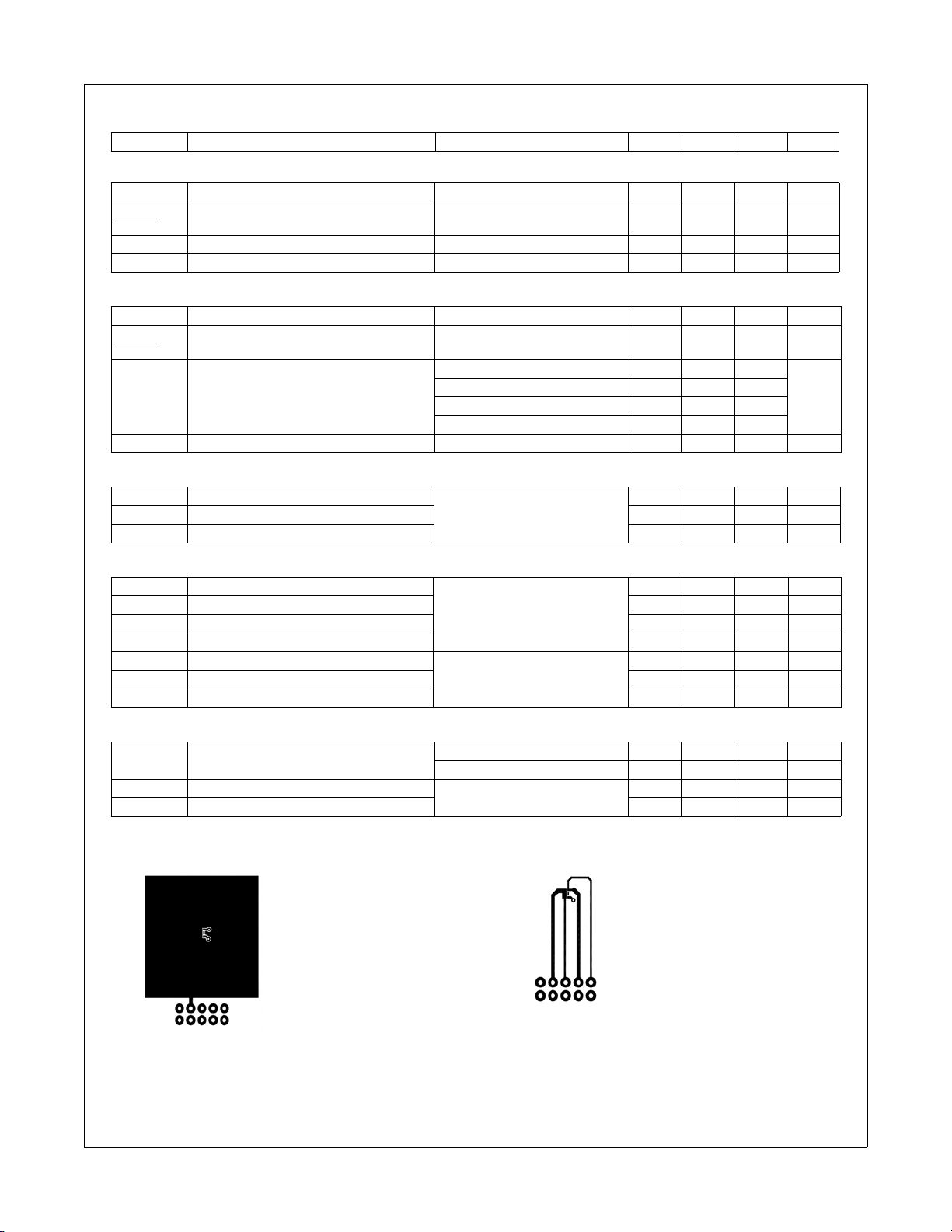
a. 60 °C/W when mounted on
a 1 in2 pad of 2 oz copper.
GS
= 0 V, IS = -1.8 A (Note 2) -0.7 -1.2 V
V
GS
= -8 A, di/dt = 100 A/μs
I
F
2
17 31 ns
is guaranteed by design while R
θJC
b. 175 °C/W when mounted on a
minimum pad of 2 oz copper.
is determined by
θCA
www.fairchildsemi.com

FDME910PZT P-Channel PowerTrench
0123
0
8
16
24
32
VGS = -2.5 V
VGS = -1.8 V
VGS = -1.5 V
VGS = - 3 V
PULSE DURATION = 80 μs
DUTY CYCLE = 0.5% MAX
VGS = -4.5 V
-I
D
, DRAIN CURRENT (A)
-V
DS
, DRAIN TO SOURCE VOLTAGE (V)
0 8 16 24 32
0
1
2
3
VGS = -1.8 V
VGS = -2.5 V
VGS = -1.5 V
PULSE DURATION = 80 μs
DUTY CYCLE = 0.5% MAX
NORMALIZED
DRAIN TO SOURCE ON-RESIST AN CE
-I
D
, DRAIN CURRENT (A)
VGS = -4.5 V
V
GS
= -3 V
-75 -50 -25 0 25 50 75 100 125 150
0.6
0.8
1.0
1.2
1.4
ID = -8 A
V
GS
= -4.5 V
NORMALIZED
DRAIN TO SOURCE ON-RESISTANCE
T
J
, JUNCTION TEMPERATURE (
o
C)
1.0 1.5 2.0 2.5 3.0 3.5 4.0 4.5
0
40
80
120
TJ = 125 oC
ID = -8 A
TJ = 25 oC
-V
GS
, GATE TO SOURCE VOLTAGE (V)
r
DS(on)
,
DRAIN TO
SOURCE ON-RESISTANCE
(mΩ)
PULSE DURATION = 80 μs
DUTY CYCLE = 0.5% MAX
0.5 1.0 1.5 2.0
0
8
16
24
32
TJ = 150 oC
V
DS
= -5 V
PULSE DURATION = 80 μs
DUTY CYCLE = 0.5% MAX
TJ = -55 oC
TJ = 25 oC
-I
D
, DRAIN CURRENT (A)
-VGS, GATE TO SOURCE V O LTAGE (V)
0.0 0.2 0.4 0.6 0.8 1.0 1.2
0.001
0.01
0.1
1
10
100
TJ = -55 oC
TJ = 25 oC
TJ = 150 oC
V
GS
= 0 V
-I
S
, REVERSE DRAIN CURRENT (A)
-VSD, BODY DIODE FORWARD VOLTAGE (V)
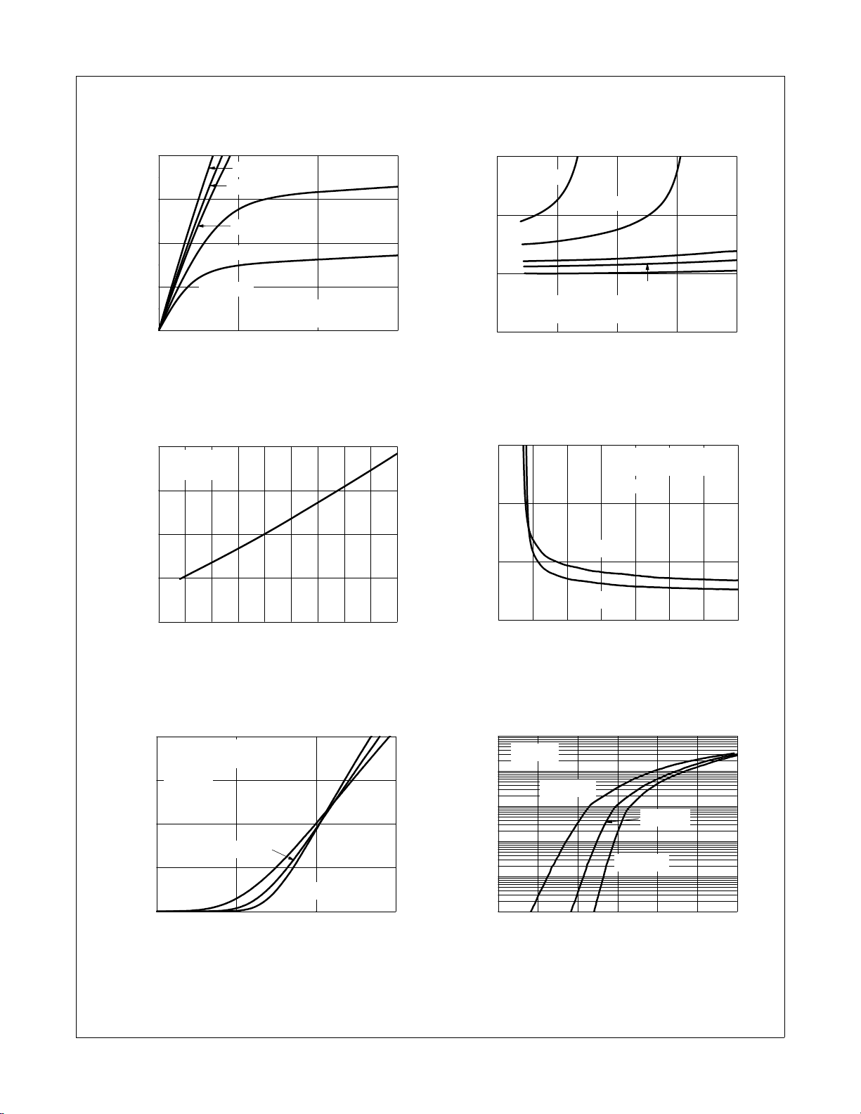
Typical Characteristics T
Figure 1.
On Region Characteristics Figure 2.
= 25 °C unless otherwise noted
J
Norm a l i z e d O n -Resistan c e
vs Drain Current and Gate Voltage
®
MOSFET
Fi g ure 3 . Nor m aliz e d On R esis t ance
vs Junction Temperature
©2012 Fairchild Semiconductor Corporation
FDME910PZT Rev.C
Figure 5. Transfer Characteristics
Figure 4.
On-Resistance vs Gate to
Source Voltage
Figure 6.
Source to Drain Diode
Forward Voltage vs Source Current
3
www.fairchildsemi.com
 Loading...