FDME1024NZT
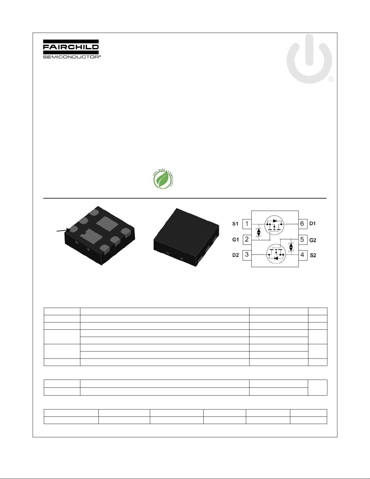
G2
S1
G1
D2
S2
D1
MicroFET 1.6x1.6 Thin
D1
D2
BOTTOM
Pin 1
TOP
Dual N-Channel PowerTrench® MOSFET
20 V, 3.8 A, 66 mΩ
Features
Max r
Max r
Max r
Max r
Low profile: 0.55 mm maximum in the new package
MicroFET 1.6x1.6 Thin
Free from halogenated compounds and antimony oxides
HBM ESD protection level > 1600 V (Note 3)
RoHS Compliant
= 66 mΩ at VGS = 4.5 V, ID = 3.4 A
DS(on)
= 86 mΩ at VGS = 2.5 V, ID = 2.9 A
DS(on)
= 113 mΩ at VGS = 1.8 V, ID = 2.5 A
DS(on)
= 160 mΩ at VGS = 1.5 V, ID = 2.1 A
DS(on)
General Description
This device is designed specifically as a single package solution
for dual switching requirement in cellular handset and other
ultra-portable applications. It features two independent
N-Channel MOSFETs with low on-state resistance for minimum
conduction losses.
The MicroFET 1.6x1.6 Thin package offers exceptional thermal
performance for it's physical size and is well suited to switching
and linear mode applications.
Applications
Baseband Switch
Load Switch
FDME1024NZT Dual N-Channel PowerTrench
July 2010
®
MOSFET
MOSFET Maximum Ratings T
Symbol Parameter Ratings Units
V
DS
V
GS
I
D
P
D
, T
T
J
STG
Thermal Characteristics
R
θJA
R
θJA
Package Marking and Ordering Information
©2010 Fairchild Semiconductor Corporation
FDME1024NZT Rev.C1
Device Marking Device Package Reel Size Tape Width Quantity
Drain to Source Voltage 20 V
Gate to Source Voltage ±8 V
Drain Current -Continuous TA = 25 °C (Note 1a) 3.8
-Pulsed 6
Power Dissipation for Single Operation TA = 25 °C (Note 1a) 1.4
Power Dissipation for Single Operation T
Operating and Storage Junction Temperature Range -55 to +150 °C
Thermal Resistance, Junction to Ambient (Single Operation) (Note 1a) 90
Thermal Resistance, Junction to Ambient (Single Operation) (Note 1b) 195
4T FDME1024NZT MicroFET 1.6x1.6 Thin 7 ’’ 8 mm 5000 units
= 25 °C unless otherwise noted
A
= 25 °C (Note 1b) 0.6
A
1
A
W
°C/W
www.fairchildsemi.com

FDME1024NZT Dual N-Channel PowerTrench
Electrical Characteristics T
= 25 °C unless otherwise noted
J
Symbol Parameter Test Conditions Min Typ Max Units
Off Characteristics
BV
DSS
ΔBV
DSS
ΔT
J
I
DSS
I
GSS
On Characteristics
V
GS(th)
ΔV
GS(th)
ΔT
J
r
DS(on)
g
FS
Drain to Source Breakdown Voltage ID = 250 μA, VGS = 0 V 20 V
Breakdown Voltage Temperature
Coefficient
Zero Gate Voltage Drain Current VDS = 16 V, V
Gate to Source Leakage Current VGS = ±8 V, V
= 250 μA, referenced to 25 °C 16 mV/°C
I
D
= 0 V 1 μA
GS
= 0 V ±10 μA
DS
Gate to Source Threshold Voltage VGS = VDS, ID = 250 μA 0.4 0.7 1.0 V
Gate to Source Threshold Voltage
Temperature Coefficient
Static Drain to Source On Resistance
Forward Transconductance VDD = 4.5 V, ID = 3.4 A 9 S
I
= 250 μA, referenced to 25 °C -3 mV/°C
D
V
= 4.5 V, ID = 3.4 A 55 66
GS
= 2.5 V, ID = 2.9 A 68 86
V
GS
= 1.8 V, ID = 2.5 A 85 113
V
GS
= 1.5 V, ID = 2.1 A 106 160
V
GS
= 4.5 V, ID = 3.4 A, TJ = 125 °C 76 112
V
GS
Dynamic Characteristics
C
iss
C
oss
C
rss
Input Capacitance
Output Capacitance 40 55 pF
Reverse Transfer Capacitance 25 40 pF
= 10 V, VGS = 0 V,
V
DS
f = 1 MHz
225 300 pF
mΩ
®
MOSFET
Switching Characteristics
t
d(on)
t
r
t
d(off)
t
f
Q
Q
Q
g
gs
gd
Turn-On Delay Time
Rise Time 2 10 ns
Turn-Off Delay Time 15 27 ns
= 10 V, ID = 1 A,
V
DD
V
= 4.5 V, R
GS
GEN
Fall Time 1.7 10 ns
Total Gate Charge
Gate to Source Gate Charge 0.4 nC
Gate to Drain “Miller” Charge 0.6 nC
= 10 V, ID = 3.4 A,
V
DD
V
= 4.5 V
GS
Drain-Source Diode Characteristics
V
SD
t
rr
Q
rr
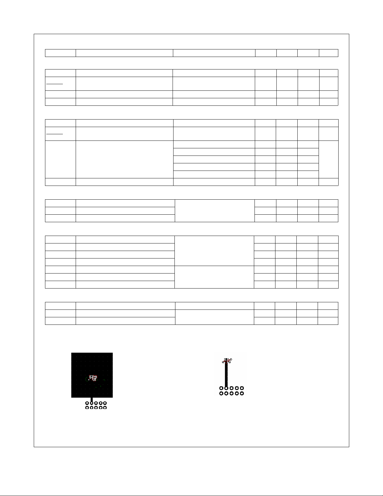
NOTES:
1. R
is determined with the device mounted on a 1 in2 pad 2 oz copper pad on a 1.5 x 1.5 in. board of FR-4 material. R
θJA
the user's board design.
Source to Drain Diode Forward Voltage V
Reverse Recovery Time
Reverse Recovery Charge 1.4 10 nC
a. 90 °C/W when mounted on
2
a 1 in
pad of 2 oz copper.
= 0 V, IS = 0.9 A (Note 2) 0.7 1.2 V
GS
= 3.4 A, di/dt = 100 A/μs
I
F
= 6 Ω
4.5 10 ns
3 4.2 nC
8.5 17 ns
is guaranteed by design while R
θJC
b. 195 °C/W when mounted on a
minimum pad of 2 oz copper.
is determined by
θCA
2. Pulse Test: Pulse Width < 300 μs, Duty cycle < 2.0%.
3. The diode connected between the gate and source serves only as protection ESD. No gate overvoltage rating is implied.
FDME1024NZT Rev.C1
2
www.fairchildsemi.com

FDME1024NZT Dual N-Channel PowerTrench
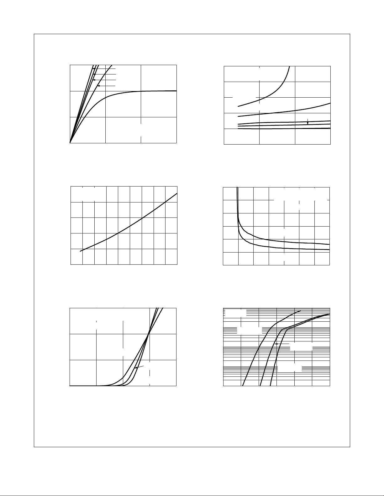
0.0 0.5 1.0 1.5
0
2
4
6
VGS = 1.8 V
VGS = 3 V
VGS = 4.5 V
VGS = 1.5 V
VGS = 2.5 V
PULSE DURATION = 80 μs
DUTY CYCLE = 0.5% MAX
I
D
, DRAIN CURRENT (A)
V
DS
, DRAIN TO SOURCE VOLTAGE (V)
0246
0.5
1.0
1.5
2.0
2.5
3.0
VGS = 2.5 V
VGS = 3 V
NORMALIZED
DRAIN TO SOURCE ON-RESISTANCE
I
D
, DRAIN CURRENT (A)
VGS = 4.5 V
VGS = 1.8 V
VGS = 1.5 V
PULSE DURATION = 80 μs
DUTY CYCLE = 0.5% MAX
-75 -50 -25 0 25 50 75 100 125 150
0.6
0.8
1.0
1.2
1.4
1.6
ID = 3.4 A
V
GS
= 4.5 V
NORMALIZED
DRAIN TO SOURCE ON-RESISTANCE
T
J
, JUNCTION TEMPERATURE (
o
C)
1.0 1.5 2.0 2.5 3.0 3.5 4.0 4.5
0
50
100
150
200
250
300
TJ = 125 oC
ID = 3.4 A
TJ = 25 oC
V
GS
, GATE TO SOURCE VOL TA G E (V)
r
DS(on)
,
DRAIN TO
SOURCE ON-RESISTANCE
(mΩ)
PULSE DURATION = 80 μs
DUTY CYCLE = 0.5% MAX
0.0 0.5 1.0 1.5 2.0
0
2
4
6
TJ = 150 oC
V
DS
= 5 V
PULSE DURATION = 80 μs
DUTY CYCLE = 0.5% MAX
TJ = -55 oC
TJ = 25 oC
I
D
, DRAIN CURRENT (A)
VGS, GATE TO SOURCE VOLTAGE (V)
0.0 0.2 0.4 0.6 0.8 1.0 1.2
0.001
0.01
0.1
1
10
TJ = -55 oC
TJ = 25 oC
TJ = 150 oC
V
GS
= 0 V
I
S
, REVERSE DRAIN CURRENT (A)
VSD, BODY DIODE FORWARD VOLTAGE (V)
Typical Characteristics T
Figure 1.
On-Region Characteristics Figure 2.
= 25 °C unless otherwise noted
J
Nor m a l i z e d On-Res i s t a n c e
vs Drain Current and Gate Voltage
®
MOSFET
Fi g u re 3. N o rmali z e d On- R e sist a n ce
vs Junction Temperature
FDME1024NZT Rev.C1
Figure 5. Transfer Characteristics
Figure 4.
On- Resistance vs Gat e to
Source Voltage
Figure 6.
Source to Drain Diode
Forward Voltage vs Source Current
3
www.fairchildsemi.com
 Loading...