February 2007
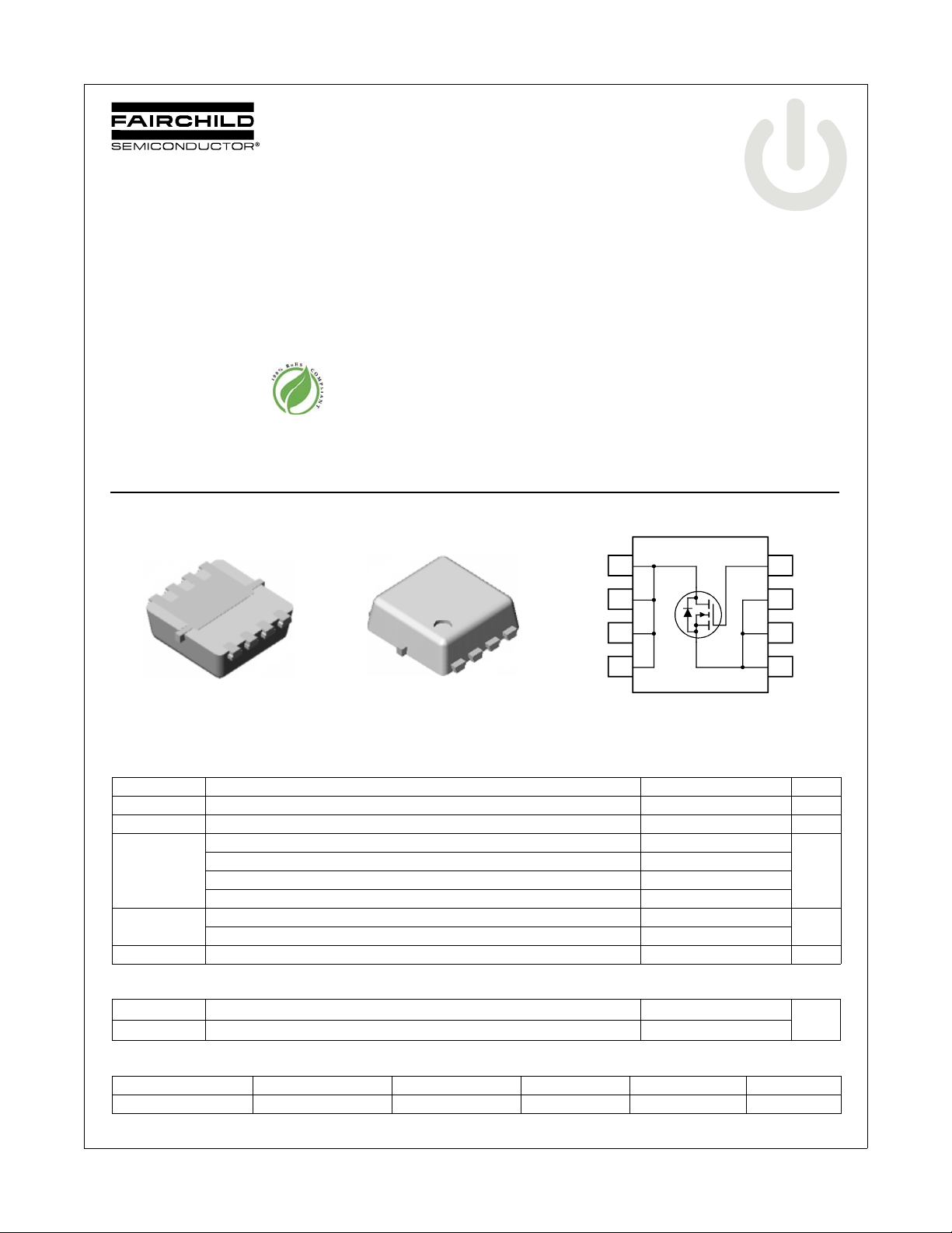
FDMC8554 N-Channel PowerTrench
FDMC8554
N-Channel Power Trench
20V, 16.5A, 5mΩ
Features
Max r
Max r
Low Profile - 1mm max in a MicroFET 3.3x3.3 mm
RoHS Compliant
= 5mΩ at VGS = 10V, ID = 16.5A
DS(on)
= 6.4mΩ at VGS = 4.5V, ID = 14A
DS(on)
Bottom
8
7
6
5
3
4
D
D
1
2
®
MOSFET
Top
D
D
General Description
This N-Channel MOSFET is a rugged gate version of
Fairchild Semiconductor‘s advanced Power Trench process.
It has been optimized for switching performance and ultra low
rdson.
Application
Synchronous rectifier
O
Ring FET
POL rectifier
G
S
S
S
tm
®
MOSFET
D
5
D
6
7
D
D
8
G
4
3
S
2
S
1
S
Power 33
MOSFET Maximum Ratings T
Symbol Parameter Ratings Units
V
DS
V
GS
I
D
P
D
, T
T
J
STG
Thermal Characteristics
R
θJC
R
θJA
Package Marking and Ordering Information
Device Marking Device Package Reel Size Tape Width Quantity
FDMC8554 FDMC8554 Power 33 7’’ 8mm 3000 units
©2007 Fairchild Semiconductor Corporation
FDMC8554 Rev.C
Drain to Source Voltage 20 V
Gate to Source Voltage ±20 V
Drain Current -Continuous (Package limited) TC = 25°C 16.5
-Continuous (Silicon limited) T
-Continuous T
-Pulsed 36
Power Dissipation TC = 25°C 41
Power Dissipation T
Operating and Storage Junction Temperature Range -55 to +150 °C
Thermal Resistance, Junction to Case 3
Thermal Resistance, Junction to Ambient (Note 1a) 60
= 25°C unless otherwise noted
A
= 25°C 72
C
= 25°C (Note 1a) 16.5
A
= 25°C (Note 1a) 2.0
A
1
A
W
°C/W
www.fairchildsemi.com

FDMC8554 N-Channel PowerTrench
Electrical Characteristics T
= 25°C unless otherwise noted
J
Symbol Parameter Test Conditions Min Typ Max Units
Off Characteristics
BV
∆BV
∆T
I
DSS
I
GSS
DSS
DSS
J
Drain to Source Breakdown Voltage ID = 250µA, VGS = 0V 20 V
Breakdown Voltage Temperature
Coefficient
Zero Gate Voltage Drain Current
Gate to Source Leakage Current VGS = ±20V, V
I
= 250µA, referenced to 25°C 15.7 mV/°C
D
V
= 16V, 1
DS
= 0V TJ = 125°C 100
V
GS
= 0V ±100 nA
DS
On Characteristics
V
GS(th)
∆V
∆T
r
DS(on)
g
FS
GS(th)
J
Gate to Source Threshold Voltage VGS = VDS, ID = 250µA 1.0 1.8 3.0 V
Gate to Source Threshold Voltage
Temperature Coefficient
Drain to Source On Resistance
I
= 250µA, referenced to 25°C -6.1 mV/°C
D
V
= 10V, ID = 16.5A 3.6 5.0
GS
= 4.5V, ID = 14A 4.6 6.4
GS
= 10V , ID = 16.5A, TJ = 125°C 5.4 7.1
V
GS
Forward Transconductance VDS = 5V, ID = 16.5A 62 S
Dynamic Characteristics
C
iss
C
oss
C
rss
R
g
Input Capacitance
Output Capacitance 795 1060 pF
Reverse Transfer Capacitance 510 765 pF
= 10V, VGS = 0V,
V
DS
f = 1MHz
Gate Resistance f = 1MHz 1.2 Ω
2540 3380 pF
mΩV
µA
®
MOSFET
Switching Characteristics
t
d(on)
t
r
t
d(off)
t
f
Q
g(TOT)
Q
g(TOT)
Q
gs
Q
gd
Turn-On Delay Time
Rise Time 10 20 ns
Turn-Off Delay Time 32 51 ns
Fall Time 714ns
Total Gate Charge at 10V
Total Gate Charge at 4.5V 24 34 nC
Gate to Source Gate Charge 8.5 nC
Gate to Drain “Miller” Charge 10 nC
VDD = 10V, ID = 16.5A
V
= 10V, R
GS
GEN
VDD = 10V, ID = 16.5A
Drain-Source Diode Characteristics
V
SD
t
rr
Q
rr
Notes:
1: R
is determined with the device mounted on a 1in2 pad 2 oz copper pad on a 1.5 x 1.5 in. board of FR-4 mat erial. R
θJA
the user's board design.
Source to Drain Diode Forward Voltage V
Reverse Recovery Time
Reverse Recovery Charge 22 33 nC
a. 60°C/W when mounted on
a 1 in2 pad of 2 oz copper
= 0V, IS = 16.5A (Note 2) 0.8 1.3 V
GS
= 16.5A, di/dt = 100A/µs
I
F
= 6Ω
13 24 ns
44 62 nC
31 47 ns
is guaranteed by design while R
θJC
b. 135°C/W when mounted on a
minimum pad of 2 oz copper
is determined by
θCA
2: Pulse Test: Pulse Width < 300µs, Duty cycle < 2.0%.
FDMC8554 Rev.C
2
www.fairchildsemi.com

FDMC8554 N-Channel PowerTrench
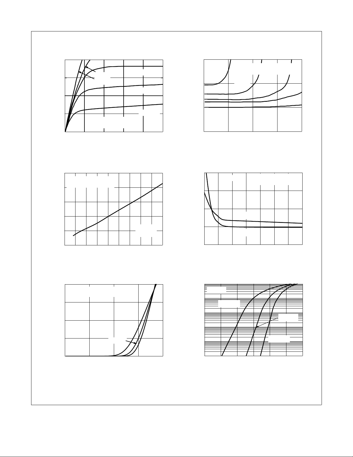
Typical Characteristics T
200
V
=5V
150
100
50
, DRAIN CURRENT (A)
D
I
0
012345
VDS, DRAIN TO SOURCE VOLTA GE (V)
Figure 1. O n - R e g i o n C h aracteristics Figure 2. N ormaliz e d O n - R e s i s t a n c e
1.6
PULSE DURATION = 80µs
DUTY CYCLE = 0.5%MAX
1.4
1.2
1.0
NORMALIZED
0.8
0.6
DRAIN TO SOURCE ON-RES ISTANCE
-75 -50 -25 0 25 50 75 100 125 150
TJ, JUNCTION TEMPERATURE (oC)
Figu r e 3 . Normal i z e d On- Res i s tance
vs Junction Temperature
100
PULSE DURATION = 80µs
DUTY CYCLE = 0.5%MAX
75
V
= 5V
DD
50
, DRAIN CURRENT ( A)
25
D
I
0
01234
VGS, GATE TO SOURCE VOLTA GE (V)
Figu re 5. Transfer Char acteristi cs Figure 6. Sourc e to Drain Diode
GS
V
= 10V
GS
PULSE DURA TION = 80µs
DUTY CYCLE = 0.5%MAX
TJ = 25oC
= 25°C unless otherwise noted
J
VGS = 4.5V
VGS = 4V
VGS = 3.5V
ID = 16.5A
V
= 10V
GS
TJ = 150oC
TJ = -55oC
3
V
= 3.5V
GS
2
PULSE DURATION = 80µs
DUTY CYCLE = 0.5%MAX
V
= 4V
GS
V
GS
=4.5V
1
NORMALIZED
0
0 50 100 150 2 00
DRAIN TO SOURCE ON-RESISTANCE
ID, DRAIN CURRENT(A)
VGS = 10V
vs Drain Current and Gate Voltage
20
ID = 16.5A
(mΩ)
15
10
, DRAIN TO
DS(on)
r
5
SOURCE ON-RESISTANCE
0
345678910
VGS, GATE TO SOURCE VOLTAGE (V)
PULSE DURATION = 80µs
DUTY CYCLE = 0.5%MAX
TJ = 125oC
TJ = 25oC
Figure 4. On-Resistance vs Gate to
Source Voltage
100
V
= 0V
GS
10
1
0.1
0.01
, REVERSE DRAIN CURRENT (A)
S
I
1E-3
0.0 0.2 0.4 0.6 0.8 1.0 1.2
TJ = 150oC
TJ = -55oC
VSD, BODY DIODE FORWARD VOLTAGE (V)
Forward Voltage vs Source Current
V
GS
TJ = 25oC
= 5V
®
MOSFET
FDMC8554 Rev.C
3
www.fairchildsemi.com
 Loading...