Fairchild FDMC7660S service manual

FDMC7660S
N-Channel Power Trench® SyncFET
30 V, 20 A, 2.2 mΩ
Features
Max r
Max r
High performance technology for extremely low r
Termination is Lead-free and RoHS Compliant
= 2.2 mΩ at VGS = 10 V, ID = 20 A
DS(on)
= 2.95 mΩ at VGS = 4.5 V, ID = 18 A
DS(on)
DS(on)
™
General Description
The FDMC7660S has been designed to minimize losses in
power conversion applications. Advancements in both silicon
and package technologies have been combined to offer the
lowest r
performance. This device has the added benefit of an efficient
monolithic Schottky body diode.
Applications
Synchronous Rectifier for DC/DC Converters
Notebook Vcore/GPU low side switch
Networking Point of Load low side switch
Telecom secondary side rectification
DS(on)
FDMC7660S N-Channel Power Trench
December 2009
while maintaining excellent switching
®
SyncFET
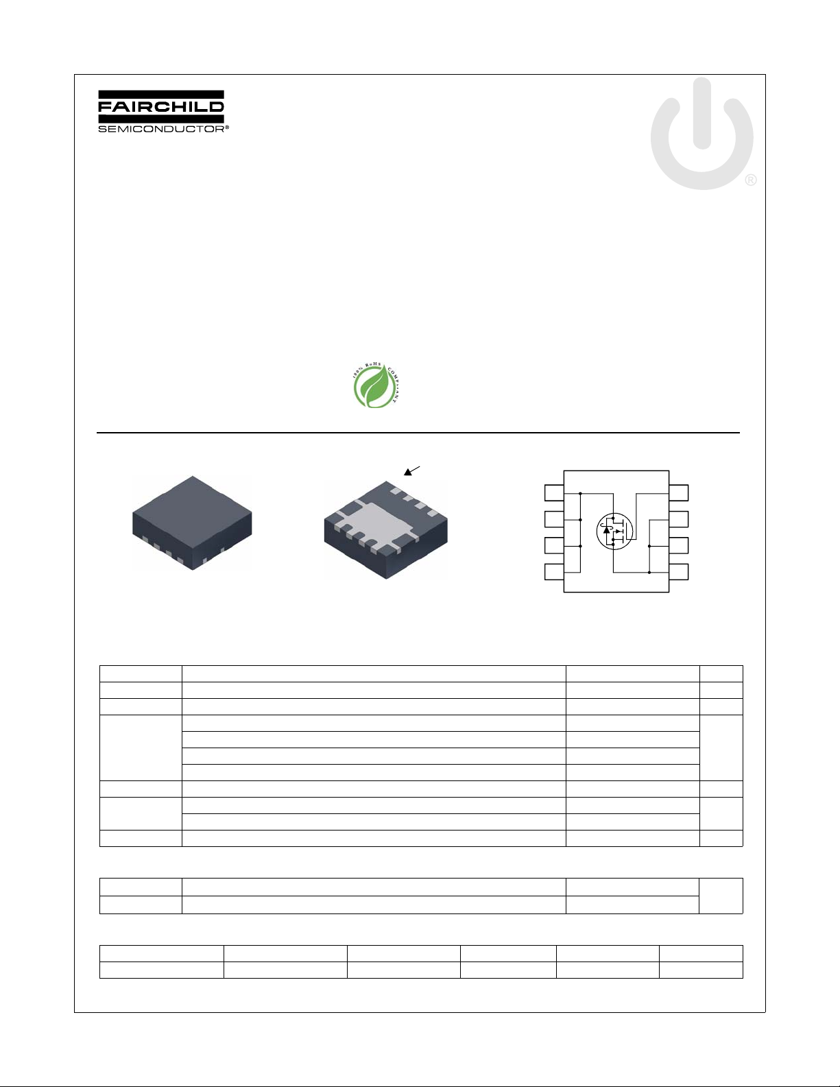
Pin 1
D
Bottom
S
S
S
G
D
5
D
6
D
7
D
8
4
3
2
1
Top
D
D
D
Power 33
MOSFET Maximum Ratings T
Symbol Parameter Ratings Units
V
DS
V
GS
I
D
E
AS
P
D
, T
T
J
STG
Drain to Source Voltage 30 V
Gate to Source Voltage (Note 4) ±20 V
Drain Current -Continuous (Package limited) TC = 25 °C 40
-Continuous (Silicon limited) T
-Continuous T
-Pulsed 200
Single Pulse Avalanche Energy (Note 3) 128 mJ
Power Dissipation 41
Power Dissipation (Note 1a) 2.3
Operating and Storage Junction Temperature Range -55 to +150 °C
= 25 °C unless otherwise noted
A
= 25 °C 100
C
= 25 °C (Note 1a) 20
A
Thermal Characteristics
™
G
S
S
S
A
W
R
θJC
R
θJA
Thermal Resistance, Junction to Case 3
Thermal Resistance, Junction to Ambient (Note 1a) 53
Package Marking and Ordering Information
Device Marking Device Package Reel Size Tape Width Quantity
FDMC7660S FDMC7660S Power 33 13 ’’ 12 mm 3000 units
©2009 Fairchild Semiconductor Corporation
FDMC7660S Rev.C
°C/W
1
www.fairchildsemi.com

FDMC7660S N-Channel Power Trench
Electrical Characteristics T
= 25 °C unless otherwise noted
J
Symbol Parameter Test Conditions Min Typ Max Units
Off Characteristics
BV
DSS
∆BV
DSS
∆T
J
I
DSS
I
GSS
On Characteristics
V
GS(th)
∆V
GS(th)
∆T
J
r
DS(on)
g
FS
Drain to Source Breakdown Voltage ID = 1 mA, VGS = 0 V 30 V
Breakdown Voltage Temperature
Coefficient
Zero Gate Voltage Drain Current VDS = 24 V, V
Gate to Source Leakage Current VGS = 20 V, V
= 1 mA, referenced to 25 °C 13 mV/°C
I
D
= 0 V 500 µA
GS
= 0 V 100 nA
DS
Gate to Source Threshold Voltage VGS = VDS, ID = 1 mA 1.2 1.6 2.5 V
Gate to Source Threshold Voltage
Temperature Coefficient
Static Drain to Source On Resistance
Forward Transconductance VDD = 5 V, ID = 20 A 129 S
I
= 1 mA, referenced to 25 °C -3 mV/°C
D
V
= 10 V, ID = 20 A 1.7 2.2
GS
= 4.5 V, ID = 18 A 2.5 2.95
GS
VGS = 10 V, ID = 20 A, TJ = 125 °C 2.2 3.1
Dynamic Characteristics
C
iss
C
oss
C
rss
R
g
Input Capacitance
Output Capacitance 1260 1680 pF
Reverse Transfer Capacitance 105 160 pF
= 15 V, VGS = 0 V,
V
DS
f = 1 MHz
3250 4325 pF
Gate Resistance 0.8 Ω
Switching Characteristics
t
d(on)
t
r
t
d(off)
t
f
Q
g(TOT)
Q
gs
Q
gd
Turn-On Delay Time
Rise Time 5 10 ns
Turn-Off Delay Time 34 54 ns
= 15 V, ID = 20 A,
V
DD
V
= 10 V, R
GS
GEN
= 6 Ω
Fall Time 3.9 10 ns
Total Gate Charge VGS = 0 V to 10 V
Total Gate Charge V
Total Gate Charge 9.5 nC
= 0 V to 4.5 V 21 29 nC
GS
V
DD
I
= 20 A
D
= 15 V
Gate to Drain “Miller” Charge 5 nC
14 25 ns
47 66 nC
mΩV
®
SyncFET
™
Drain-Source Diode Characteristics
V
= 0 V, IS = 20 A (Note 2) 0.8 1.2
V
SD
t
rr
Q
rr
NOTES:
is determined with the device mounted on a 1in2 pad 2 oz copper pad on a 1.5 x 1.5 in. board of FR- 4 mat erial . R
1. R
θJA
the user's board design.
2. Pulse Test: Pulse Width < 300 µs, Duty cycle < 2.0 %.
3. Starting TJ = 25oC; N-ch: L = 1 mH, IAS = 16 A, VDD = 27 V, VGS = 10 V.
4. As an N-ch device, the negative Vgs rating is for low duty cycle pulse ocurrence only. No continuous rating is implied.
©2009 Fairchild Semiconductor Corporation
FDMC7660S Rev.C
Source to Drain Diode Forward Voltage
Reverse Recovery Time
Reverse Recovery Charge 39 62 nC
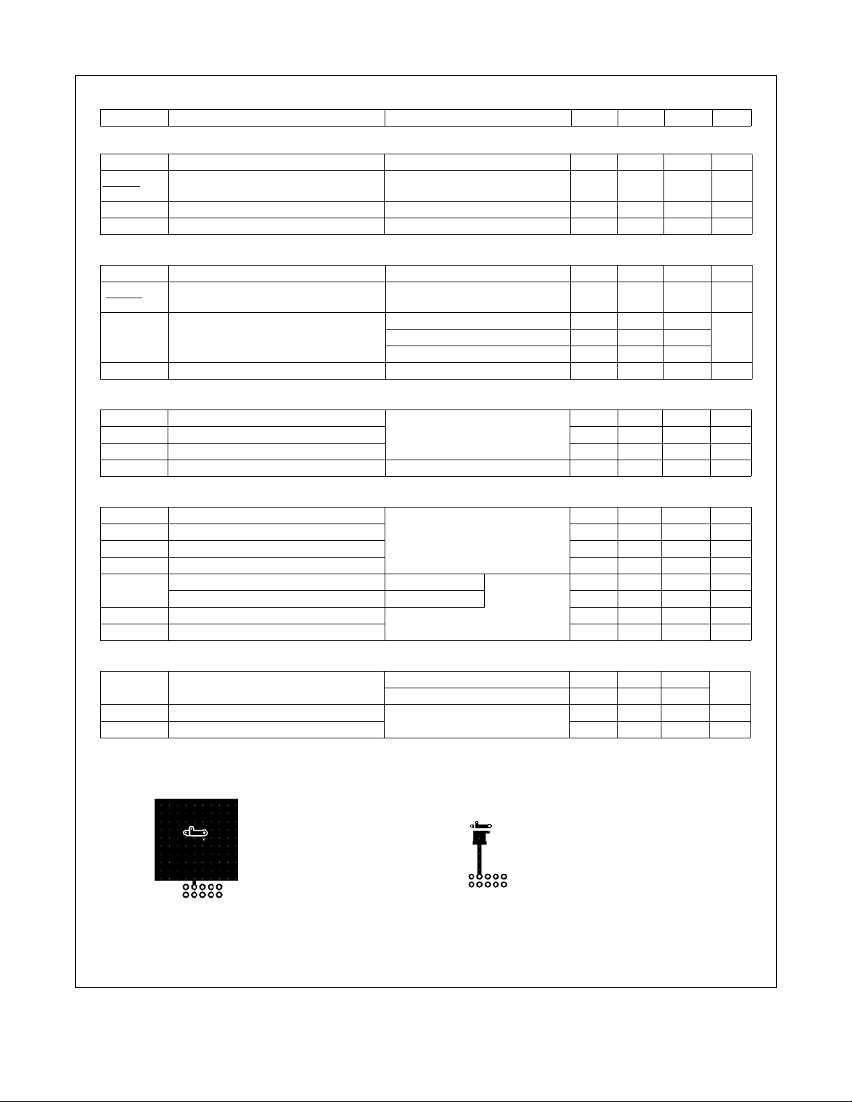
a. 53°C/W when mounted on
a 1 i n2 pad o f 2 oz c o pper
GS
= 0 V, IS = 1.9 A (Note 2) 0.4 0.7
V
GS
= 20 A, di/dt = 300 A/µs
I
F
2
31 50
is guaranteed by design while R
θJC
b. 125°C/W when mounted on a
minimum pad of 2 oz copper
V
ns
is determined by
θCA
www.fairchildsemi.com

FDMC7660S N-Channel Power Trench
Typical Characteristics T
200
VGS = 10 V
150
100
DRAIN CURRENT (A)
50
,
D
I
0
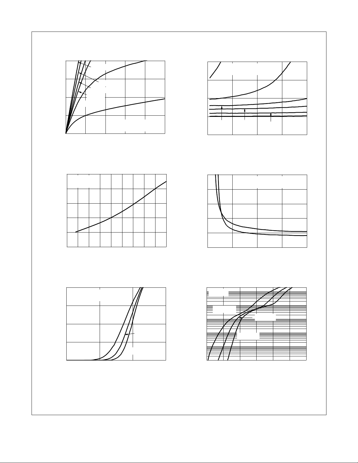
0.0 0.5 1.0 1.5 2.0 2.5
Figure 1.
1.6
ID = 20 A
= 10 V
V
GS
1.4
1.2
1.0
NORMALIZED
0.8
DRAIN TO SOURCE ON-RESISTANCE
0.6
-75 -50 -25 0 25 50 75 100 125 150
Figure 3. N o r m a l i z ed On- Resista n c e
vs Junction Temperature
VGS = 6 V
VGS = 4.5 V
VGS = 4 V
VGS = 3.5 V
VGS = 3 V
V
,
DRAIN TO SOURCE VOLTAGE (V)
DS
PULSE DURATION = 80 µs
DUTY CYCLE = 0.5% MAX
On-Region Characteristics Figure 2.
T
,
JUNCTION TEMPERATURE
J
= 25 °C unless otherwise noted
J
o
(
C
)
4
PULSE DURATION = 80 µs
DUTY CYCLE = 0.5% MAX
3
VGS = 3 V
VGS = 3.5 V
2
NORMALIZED
1
VGS = 4 V
DRAIN TO SOURCE ON-RESISTANCE
0
0 50 100 150 200
VGS = 4.5 V
I
,
DRAIN CURRENT (A)
D
VGS = 6 V
VGS = 10 V
Norm a l i zed O n - R esis t a n ce
vs Drain Current and Gate Voltage
10
)
Ω
m
8
(
6
DRAIN TO
,
4
DS(on)
r
2
SOURCE ON-RESISTANCE
0
246810
Figure 4.
TJ = 25 oC
V
,
GATE TO SOURCE VOLTAGE (V)
GS
On-R esistance vs Gate to
PULSE DURATION = 80 µs
DUTY CYCLE = 0.5% M AX
ID = 20 A
TJ = 125 oC
Source Voltage
®
SyncFET
™
200
PULSE DURATION = 80 µs
DUTY CYCLE = 0.5% MAX
150
V
= 5 V
DS
100
50
, DRAIN CURRENT (A)
D
I
0
1234
VGS, GATE TO SOURCE VOLTAGE (V)
TJ = 125 oC
Figure 5. Transfer Characteristics
©2009 Fairchild Semiconductor Corporation
FDMC7660S Rev.C
TJ = 25 oC
TJ = -55 oC
200
100
V
= 0 V
GS
10
TJ = 125 oC
1
TJ = 25 oC
0.1
0.01
, REVERSE DRAIN CURRENT (A)
S
I
0.001
0.0 0.2 0.4 0.6 0.8 1.0 1.2
VSD, BODY DIODE FORWARD VOLTAGE (V)
Figure 6.
TJ = -55 oC
Source to Drain Diode
Forward Voltage vs Source Current
3
www.fairchildsemi.com
 Loading...