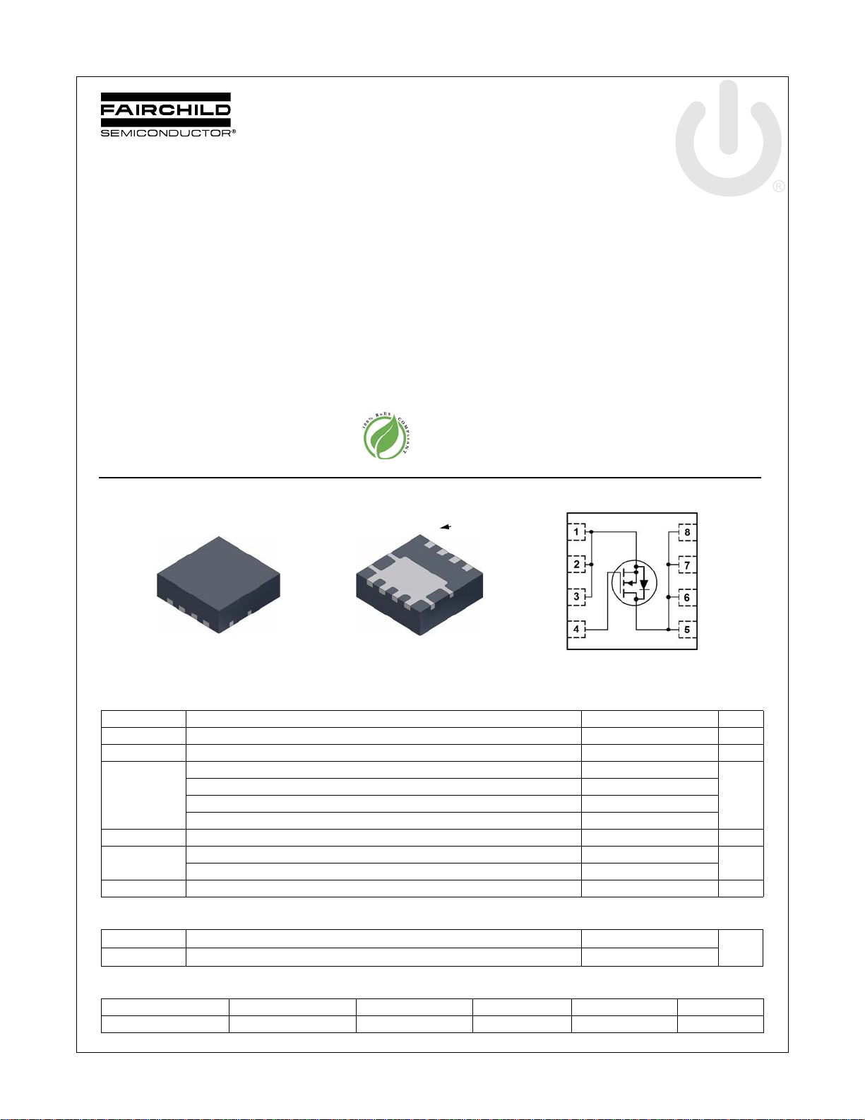
FDMC7582
S
S
S
G
D
D
D
D
Top
Power 33
Bottom
D
D
D
D
S
S
S
G
Pin 1
N-Channel PowerTrench® MOSFET
25 V, 49 A, 5.0 mΩ
Features
Max r
Max r
State-of-the-art switching performance
Lower output capacitance, gate resistance, and gate charge
boost efficiency
Shielded gate technology reduces switch node ringing and
increases immunity to EMI and cross conduction
Clip bonding technology further reduces On resistance and
source inductance
RoHS Compliant
= 5.0 mΩ at VGS = 10 V, ID = 16.7 A
DS(on)
= 7.5 mΩ at VGS = 4.5 V, ID = 13.6 A
DS(on)
General Description
This N-Channel MOSFET has been designed specifically to
improve the overall efficiency and to minimize switch node
ringing of DC/DC converters using either synchronous or
conventional switching PWM controllers. It has been optimized
for low gate charge, low r
diode reverse recovery performance.
Application
High side switching for high end computing
High power density DC-DC synchronous buck
Low loss load switch
Communication & telecon Point of Load
FDMC7582 N-Channel PowerTrench
April 2012
DS(on), fast switching speed and body
.
®
MOSFET
MOSFET Maximum Ratings T
Symbol Parameter Ratings Units
V
DS
V
GS
I
D
E
AS
P
D
, T
T
J
STG
Thermal Characteristics
R
θJC
R
θJA
Package Marking and Ordering Information
Device Marking Device Package Reel Size Tape Width Quantity
FDMC7582 FDMC7582 Power 33 13 ’’ 12 mm 3000 units
©2012 Fairchild Semiconductor Corporation
FDMC7582 Rev.C6
Drain to Source Voltage 25 V
Gate to Source Voltage (Note 3) ±20 V
Drain Current - Continuous (Package limited) Tc=25C 49
- Continuous (Silicon Limited) Tc=25C 76
- Continuous T
- Pulsed 60
Single Pulse Avalanche Energy (Note 4) 38 mJ
Power Dissipation TC = 25 °C 52
Power Dissipation T
Operating and Storage Junction Temperature Range -55 to +150 °C
Thermal Resistance, Junction to Case 2.4
Thermal Resistance, Junction to Ambient (Note 1a) 53
= 25 °C unless otherwise noted
A
= 25 °C (Note 1a) 16.7
A
= 25 °C (Note 1a) 2.3
A
1
A
W
°C/W
www.fairchildsemi.com

FDMC7582 N-Channel PowerTrench
Electrical Characteristics T
= 25 °C unless otherwise noted
J
Symbol Parameter Test Conditions Min Typ Max Units
Off Characteristics
BV
ΔBV
ΔT
I
DSS
I
GSS
DSS
DSS
J
Drain to Source Breakdown Voltage ID = 250 μA , VGS = 0 V 25 V
Breakdown Voltage Temperature
Coefficient
Zero Gate Voltage Drain Current VDS = 20 V, V
Gate to Source Leakage Current, Forward VGS = 20 V, V
I
= 250 μA , referenced to 25 °C 19 mV/°C
D
= 0 V 1 μA
GS
= 0 V 100 nA
DS
On Characteristics
V
GS(th)
ΔV
ΔT
r
DS(on)
g
FS
GS(th)
J
Gate to Source Threshold Voltage VGS = VDS, ID = 250 μA 1.2 1.7 2.5 V
Gate to Source Threshold Voltage
Temperature Coefficient
Static Drain to Source On Resistance
I
= 250 μA , referenced to 25 °C -5 mV/°C
D
V
= 10 V, ID = 16.7 A 4.0 5.0
GS
= 4.5 V, ID = 13.6 A 6.0 7.5
GS
= 10 V, ID = 16.7 A,TJ = 125 °C 5.4 7.0
V
GS
Forward Transconductance VDD = 5 V, ID = 16.7 A 58 S
Dynamic Characteristics
C
iss
C
oss
C
rss
R
g
Input Capacitance
Output Capacitance 372 495 pF
Reverse Transfer Capacitance 79 120 pF
Gate Resistance 0.1 0.9 2.9 Ω
Switching Characteristics
t
d(on)
t
r
t
d(off)
t
f
Q
g(TOT)
Q
g(TOT)
Q
gs
Q
gd
Turn-On Delay Time
Rise Time 210ns
Turn-Off Delay Time 20 36 ns
Fall Time 1.6 10 ns
Total Gate Charge at 10V
Total Gate Charge at 4.5V 9.5 13 nC
Total Gate Charge 3.9 nC
Gate to Drain “Miller” Charge 2.5 nC
= 13 V, VGS = 0 V,
V
DS
f = 1 MHz
= 13 V, ID = 16.7A,
V
DD
V
= 10 V, R
GS
V
= 13 V, ID = 16.7 A
DD
GEN
= 6 Ω
1348 1795 pF
8.8 18 ns
20 28 nC
mΩV
®
MOSFET
Drain-Source Diode Characteristics
V
= 0 V, IS = 16.7 A (Note 2) 0.8 1.3 V
V
SD
t
rr
Q
rr
Notes:
1. R
is determined with the device mounted on a 1in2 pad 2 oz copper pad on a 1.5 x 1.5 in. board of FR-4 mate rial. R
θJA
the user's board design.
2. Pulse Test: Pulse Width < 300 μs, Duty cycle < 2.0%.
3. As an N-ch device, the negative Vgs rating is for low duty cycle pulse ocurrence only. No continuous rating is implied.
4. E
AS of 38 mJ is based on starting TJ = 25 oC; N-ch: L = 0.3 mH, IAS = 16 A, VDD = 23 V, VGS = 10 V.
©2012 Fairchild Semiconductor Corporation
FDMC7582 Rev.C6
Source to Drain Diode Forward Voltage
Reverse Recovery Time
Reverse Recovery Charge 7 14 nC
a.
53 °C/W when mounted on a
1 in2 pad of 2 oz copper
SS
SF
DS
DF
G
GS
= 0 V, IS = 2 A (Note 2) 0.7 1.2
V
GS
= 16.7 A, di/dt = 100 A/μs
I
F
2
22 39 ns
is guaranteed by design while R
θJC
b.
125 °C/W when mounted on
a minimum pad of 2 oz copper
SS
SF
DF
DS
G
is determined by
θCA
www.fairchildsemi.com

FDMC7582 N-Channel PowerTrench
0123
0
10
20
30
40
50
60
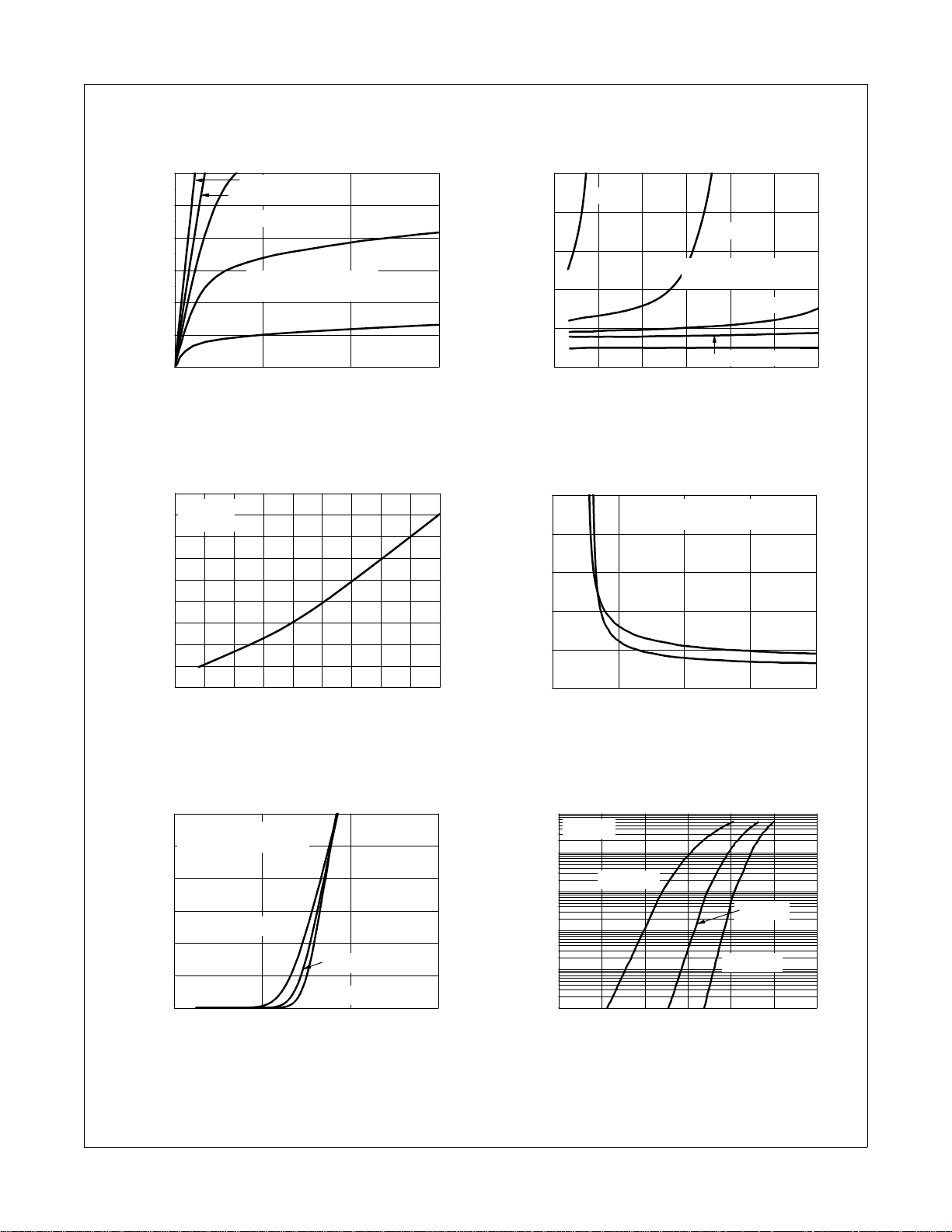
VGS = 3 V
VGS = 3.5 V
VGS = 4 V
PULSE DURA TION = 80 μs
DUTY CYCLE = 0.5% MAX
VGS = 5 V
VGS = 10 V
I
D
, DRAIN CURRENT (A)
V
DS
, DRAIN TO SOURCE VOLTAGE (V)
0 102030405060
0
2
4
6
8
10
VGS = 3 V
VGS = 5 V
PULSE DURA TION = 80 μs
DUTY CYCLE = 0.5% MAX
NORMALIZED
DRAIN TO SOURCE ON-RESISTA NCE
I
D
, DRAIN CURRENT (A)
VGS = 3.5 V
VGS = 4 V
V
GS
= 10 V
-75 -50 -25 0 25 50 75 100 125 150
0.7
0.8
0.9
1.0
1.1
1.2
1.3
1.4
1.5
1.6
ID = 16.7 A
V
GS
= 10 V
NORMALIZED
DRAIN TO SOURCE ON-RESIST ANCE
T
J
, JUNCTION TE MPERATURE (
o
C)
246810
0
6
12
18
24
30
TJ = 125 oC
ID = 16.7 A
TJ = 25 oC
V
GS
, GATE TO SOURCE VOLTA G E (V)
r
DS(on)
,
DRAIN TO
SOURCE ON-RESISTANCE
(mΩ)
PULSE DURATION = 80 μs
DUTY CYCLE = 0.5% MAX
0246
0
10
20
30
40
50
60
TJ = 150 oC
V
DS
= 5 V
PULSE DURATION = 80 μs
DUTY CYCLE = 0.5% MAX
TJ = -55 oC
TJ = 25 oC
I
D
, DRAIN CURRENT (A)
VGS, GATE TO SOURCE VOLTAGE (V)
0.0 0.2 0.4 0.6 0.8 1.0 1.2
0.001
0.01
0.1
1
10
100
TJ = -55 oC
TJ = 25 oC
TJ = 150 oC
V
GS
= 0 V
I
S
, REVERSE DRAIN CURRENT (A)
VSD, BODY DIODE FORWARD VOLTAGE (V)
Typical Characteristics T
Figure 1.
On Region Characteristics Figure 2.
= 25°C unless otherwise noted
J
®
MOSFET
Nor mal ized O n-R esi sta nce
vs Drain Current and Gate Voltage
Figure 3. N or ma lized On Re si stance
vs Junction Temperature
©2012 Fairchild Semiconductor Corporation
FDMC7582 Rev.C6
Figure 5. Transfer Characteristics
Figure 4.
On-Resistance vs Ga te to
Source Voltage
Figure 6.
Source to D rain Diode
Forward Voltage vs Source Current
3
www.fairchildsemi.com
 Loading...