Fairchild FDMC6679AZ service manual

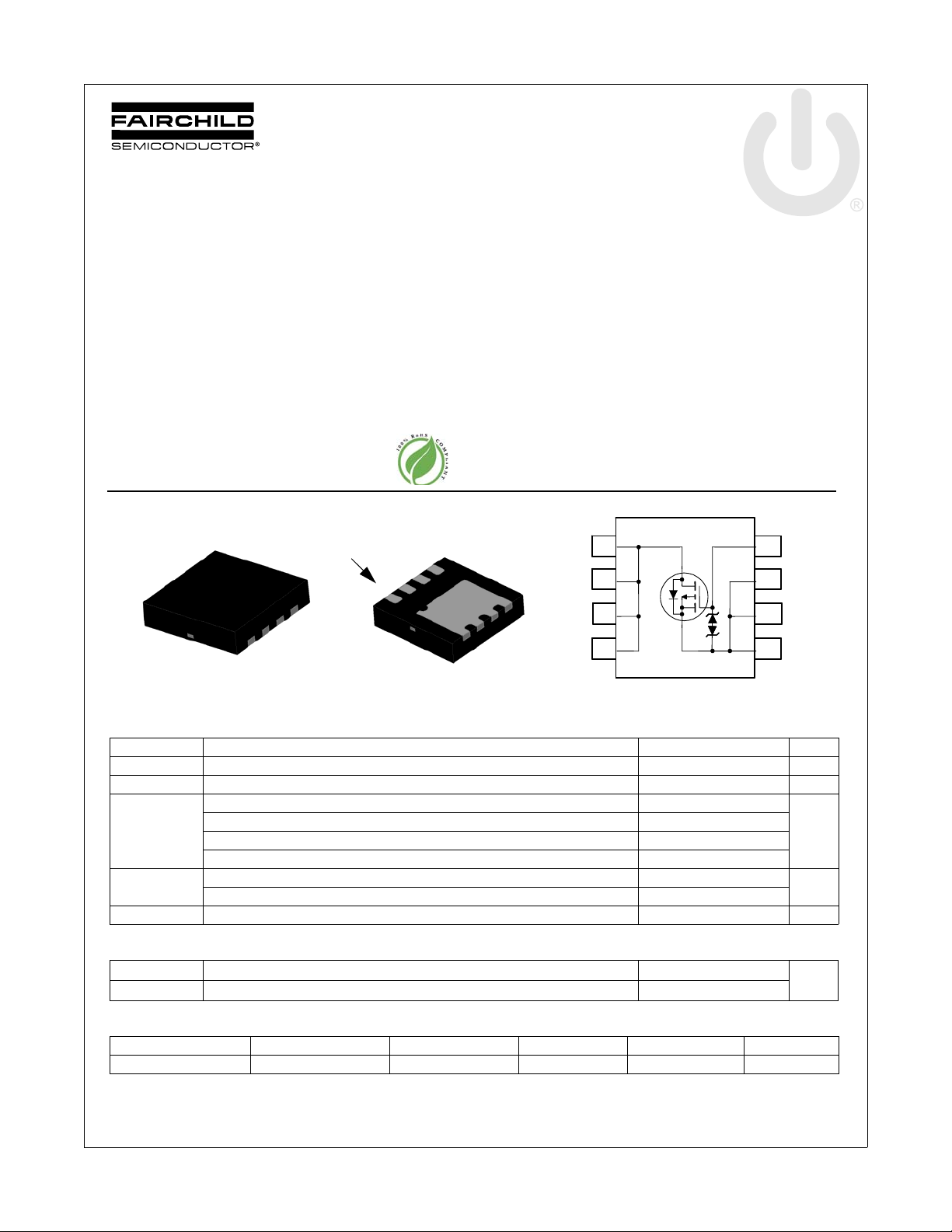
FDMC6679AZ
P-Channel PowerTrench® MOSFET
-30 V, -20 A, 10 mΩ
Features
Max r
Max r
HBM ESD protection level of 8 kV typical(note 3)
Extended V
High performance trench technology for extremely low r
High power and current handling capability
Termination is Lead-free and RoHS Compliant
= 10 mΩ at VGS = -10 V, ID = -11.5 A
DS(on)
= 18 mΩ at VGS = -4.5 V, ID = -8.5 A
DS(on)
range (-25 V) for battery applications
GSS
DS(on)
General Description
The FDMC6679AZ has been designed to minimize losses in
load switch applications. Advancements in both silicon and
package technologies have been combined to offer the lowest
r
and ESD protection.
DS(on)
Applications
Load Switch in Notebook and Server
Notebook Battery Pack Power Management
FDMC6679AZ P-Channel PowerTrench
July 2009
®
MOSFET
Top
Pin 1
S
Bottom
5
G
S
S
D
D
D
D
D
6
D
7
D
8
D
4
3
2
1
MLP 3.3x3.3
MOSFET Maximum Ratings T
Symbol Parameter Ratings Units
V
DS
V
GS
I
D
P
D
, T
T
J
STG
Drain to Source Voltage -30 V
Gate to Source Voltage ±25 V
Drain Current -Continuous (Package limited) TC = 25 °C -20
-Continuous (Silicon limited) T
-Continuous T
-Pulsed -32
Power Dissipation TC = 25 °C 41
Power Dissipation T
Operating and Storage Junction Temperature Range -55 to +150 °C
= 25 °C unless otherwise noted
A
= 25 °C -51
C
= 25 °C (Note 1a) -11.5
A
= 25 °C (Note 1a) 2.3
A
Thermal Characteristics
G
S
S
S
A
W
R
θJC
R
θJA
Thermal Resistance, Junction to Case 3
Thermal Resistance, Junction to Ambient (Note 1a) 53
Package Marking and Ordering Information
Device Marking Device Package Reel Size Tape Width Quantity
FDMC6679AZ FDMC6679AZ MLP 3.3x3.3 13 ’’ 12 mm 3000 units
©2009 Fairchild Semiconductor Corporation
FDMC6679AZ Rev.D1
°C/W
1
www.fairchildsemi.com

FDMC6679AZ P-Channel PowerTrench
Electrical Characteristics T
= 25 °C unless otherwise noted
J
Symbol Parameter Test Conditions Min Typ Max Units
Off Characteristics
BV
∆BV
∆T
I
DSS
I
GSS
DSS
DSS
J
Drain to Source Breakdown Voltage ID = -250 µA, VGS = 0 V -30 V
Breakdown Voltage Temperature
Coefficient
Zero Gate Voltage Drain Current
Gate to Source Leakage Current VGS = ±25 V, V
I
= -250 µA, referenced to 25 °C 29 mV/°C
D
V
= -24 V, -1
DS
= 0 V, TJ = 125 °C -100
V
GS
= 0 V ±10 µA
DS
On Characteristics
V
GS(th)
∆V
∆T
r
DS(on)
g
FS
GS(th)
J
Gate to Source Threshold Voltage VGS = VDS, ID = -250 µA-1-1.8-3V
Gate to Source Threshold Voltage
Temperature Coefficient
Static Drain to Source On Resistance
I
= -250 µA, referenced to 25 °C -7 mV/°C
D
V
= -10 V, ID = -11.5 A 8.6 10
GS
= -4.5 V, ID = -8.5 A 12 18
GS
= -10 V , ID = -11.5 A, TJ = 125 °C 12 15
V
GS
Forward Transconductance VDS = -5 V, ID = -11.5 A 46 S
Dynamic Characteristics
C
iss
C
oss
C
rss
R
g
Input Capacitance
Output Capacitance 570 755 pF
Reverse Transfer Capacitance 500 750 pF
= -15 V, VGS = 0 V,
V
DS
f = 1 MHz
Gate Resistance 4.3 Ω
2985 3970 pF
µA
mΩV
®
MOSFET
Switching Characteristics
t
d(on)
t
r
t
d(off)
t
f
Q
Q
Q
Q
g
g
gs
gd
Turn-On Delay Time
Rise Time 14 25 ns
Turn-Off Delay Time 63 100 ns
Fall Time 46 73 ns
Total Gate Charge VGS = 0 V to -10 V
Total Gate Charge VGS = 0 V to -5 V 37 52 nC
Gate to Source Charge 8.7 nC
Gate to Drain “Miller” Charge 17 nC
= -15 V, ID = -11.5 A,
V
DD
V
= -10 V, R
GS
GEN
= 6 Ω
Drain-Source Diode Characteristics
V
= 0 V, IS = -11.5 A (Note 2) 0.83 1.30
V
SD
t
rr
Q
rr
NOTES:
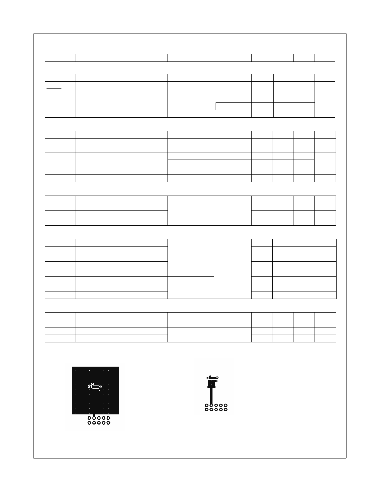
is determined with the device mounted on a 1 in2 pad 2 oz copper pad on a 1.5 x 1.5 in. board of FR-4 material. R
1. R
θJA
the user's board design.
Source to Drain Diode Forward Voltage
Reverse Recovery Time
Reverse Recovery Charge 16 28 nC
a. 53 °C/W when mounted on
a 1 in2 pad of 2 oz copper
GS
= 0 V, IS = -1.6 A (Note 2) 0.71 1.20
V
GS
= -11.5 A, di/dt = 100 A/µs
I
F
= -15 V,
V
DD
I
= -11.5 A
D
12 21 ns
65 91 nC
31 49 ns
is guaranteed by design while R
θJC
b.125 °C/W when mounted on
a minimum pad of 2 oz copper
is determined by
θCA
V
2. Pulse Test: Pulse Width < 300 µs, Duty cycle < 2.0 %.
3. The diode connected bet ween the gate and source servers only as protection against ESD. No gate overvoltage rating is implied.
©2009 Fairchild Semiconductor Corporation
FDMC6679AZ Rev.D1
2
www.fairchildsemi.com

FDMC6679AZ P-Channel PowerTrench
Typical Characteristics T
32
24
16
, DRAIN CURRENT (A)
8
D
-I
0
0123
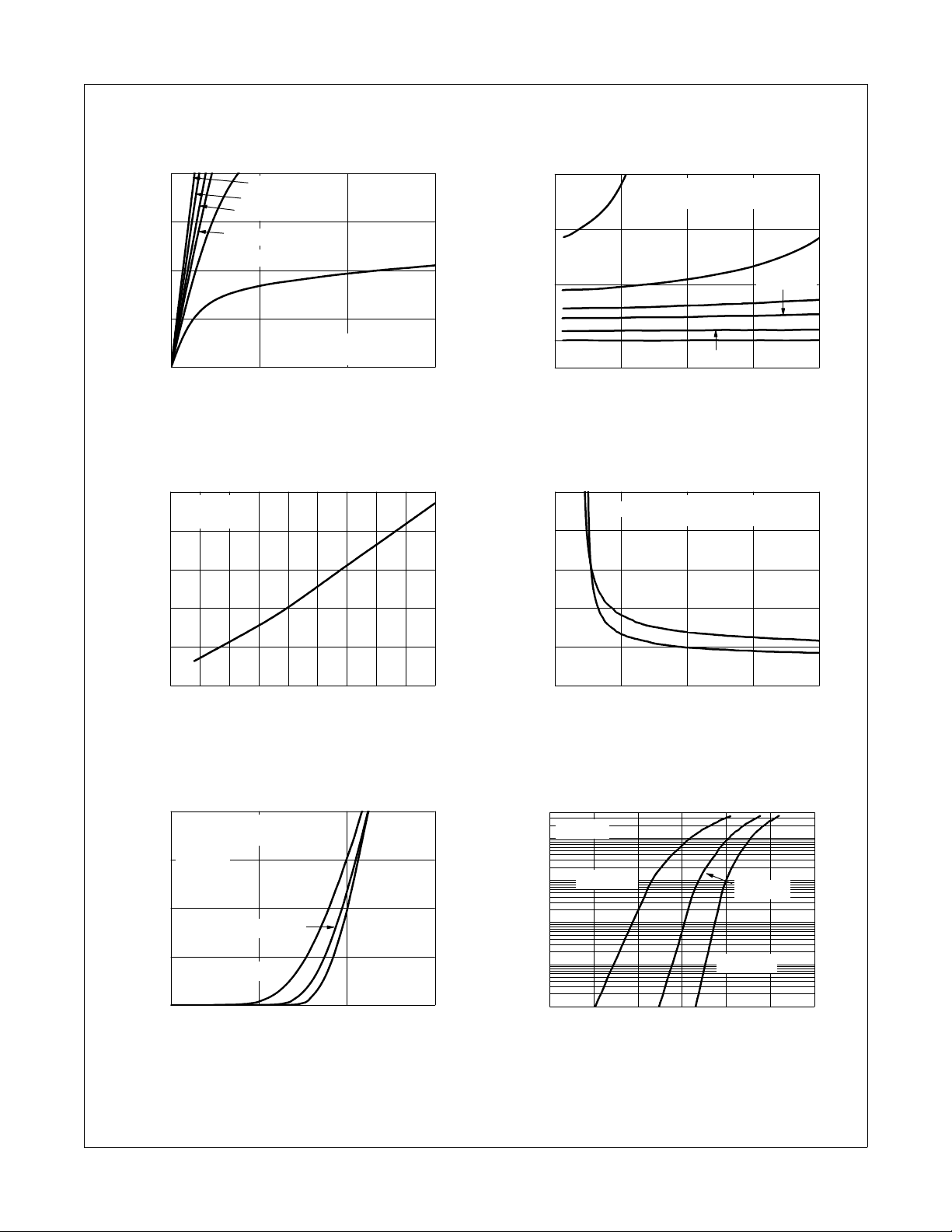
Figure 1.
1.6
ID = -11.5 A
V
= -10 V
GS
1.4
1.2
1.0
NORMALIZED
0.8
DRAIN TO SOURCE ON-RESISTANCE
0.6
-75 -50 -25 0 25 50 75 100 125 150
VGS = -10 V
VGS = -6 V
VGS = -4.5 V
VGS = -4 V
VGS = -3.5 V
PULSE DURATION = 80 µs
DUTY CYCLE = 0.5% MAX
-V
, DRAIN TO SOURCE VOLTAGE (V)
DS
On Region Characteristics Figure 2.
T
, JUNCTION TEMPERATURE (
J
= 25 °C unless otherwise noted
J
VGS = -3 V
o
C)
4
VGS = -3 V
PULSE DURATION = 80 µs
DUTY CYCLE = 0.5% MAX
3
VGS = -3.5 V
2
NORMALIZED
V
= -4 V
GS
VGS = -4.5 V
1
V
= -10 V
DRAIN TO SOURCE ON-RESISTANCE
VGS = -6 V
GS
0 8 16 24 32
-I
, DRAIN CURRENT (A)
D
Nor m a l i z e d On-Resis t a n c e
vs Drain Current and Gate Voltage
50
ID = -11.5 A
40
(mΩ)
30
DRAIN TO
,
20
DS(on)
r
10
SOURCE ON-RESISTANCE
0
246810
TJ = 25 oC
-V
, GATE TO SOURCE VOL TA G E (V)
GS
PULSE DURATION = 80 µs
DUTY CYCLE = 0.5% MAX
TJ = 125 oC
®
MOSFET
Fi gure 3 . No r mali zed O n Res i sta n ce
vs Junction Temperature
32
PULSE DURATION = 80 µs
DUTY CYCLE = 0.5% MAX
V
= -5 V
24
DS
16
8
, DRAIN CURRENT (A)
D
-I
0
1234
TJ = 25 oC
TJ = 150 oC
-VGS, GATE TO SOURCE VOLTAGE (V)
Figure 5. Transfer Characteristics
©2009 Fairchild Semiconductor Corporation
FDMC6679AZ Rev.D1
Figure 4.
On-Re sistance v s Gate to
Source Voltage
40
V
= 0 V
GS
10
TJ = 150 oC
1
TJ = -55 oC
0.1
0.01
, REVERSE DRAIN CURRENT (A)
S
-I
0.001
0.0 0.2 0.4 0.6 0.8 1.0 1.2
-VSD, BODY DIODE FORWARD VOLTAGE (V)
Figure 6.
Sou rce to Drain Diode
TJ = 25 oC
TJ = -55 oC
Forward Voltage vs Source Current
3
www.fairchildsemi.com
 Loading...